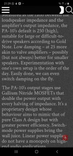
Papa or anyone played with this yet?
It sounded wow blow me down.. On one commercial amp.. I squeal with excitement like a girl.
It sounded wow blow me down.. On one commercial amp.. I squeal with excitement like a girl.
Papa or anyone played with this yet?
It sounded wow blow me down.. On one commercial amp.. I squeal with excitement like a girl.
Can you name the amplifier? It would be interesting to see.
I presume it's a Class D switching amp, and GaN make for excellent switches.
My advice, don't try to use them in linear applications as the ones I have
played with don't have any kind of DC safe operating area. I have blown
up a few trying to run them at 20 volts / 1 amp.

My advice, don't try to use them in linear applications as the ones I have
played with don't have any kind of DC safe operating area. I have blown
up a few trying to run them at 20 volts / 1 amp.

GaN in the linear region would be very slippery and prone to squealing in high soprano. It's the solid state equivalent of those tubes that "oscillate in the box".
Papa is right - they are excellent switches.
Papa is right - they are excellent switches.
In my case I did not see any oscillation, so I put it down to the development
of hot spots on the die. That has definitely been an issue with silicon switching
transistors, such that many no longer specify a DC safe operating area.
of hot spots on the die. That has definitely been an issue with silicon switching
transistors, such that many no longer specify a DC safe operating area.
When GaN devices oscillate, they like to do so in the multi-hundred MHz - GHz region. GaN HEMTs are the bee's knees and the dog's bollocks for microwave applications. One person has suggested replacing the magnetron in a microwave oven with a number of GaN HEMTs, but at the current stage of development, that would be one pricey microwave...
I wonder if the amp guys were using the EPC GaN mosfets for their Class D app. We tried them at my work, and they make wonderful synchronous rectifiers. However, since they only come as bumped die, they are a royal pain in the butt to solder unless you have a full pick n' place/IR reflow setup. We were hand soldering the devices, and we had to take them downstairs to QA and X-ray the boards to make sure the bumps were lined up with the pads. It was an experiment we only tried once...
The input capacitance of GaN is much lower than that of SiC. This makes them switch very fast. They also can have very low on resistance at high temperature.
On the downside, they trap electrons if stood off at high voltage. This makes on resistance high for a microsecond or two and creates a switching loss.
The day job has bumped up against SiC and GaN. Met some people who have dabbled in SiC SITs during the early days of SiC years ago.
On the downside, they trap electrons if stood off at high voltage. This makes on resistance high for a microsecond or two and creates a switching loss.
The day job has bumped up against SiC and GaN. Met some people who have dabbled in SiC SITs during the early days of SiC years ago.
Last edited:
We deal with all that stuff with the GaN devices we sell in the products marketed at my job. It's an issue for HV GaN devices, (~650V is the transition point of concern) - not so much for lower voltage devices. I was somewhat pessimistic about my company's involvement with GaN, but it has worked out way beyond my expectations.
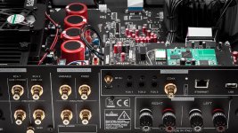
View attachment 882291
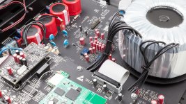
View attachment 882292
Any idea what the final transistor is? Is 1000 goldnote
Looks like chip amp to me but could not confirm. Notes say mosfet
Man I want red capacitors in my amps! 😀 (sorry for the off topic
 )
)My advice, don't try to use them in linear applications as the ones I have
played with don't have any kind of DC safe operating area. I have blown
up a few trying to run them at 20 volts / 1 amp.
I'm glad I read this before making a purchase. I saw these GaN FETs and started thinking about an F1G, but I will look at other options instead.
The Transphorm devices are likely not pure GaN fets, but instead a low voltage Silicon mosfet cascoded with a GaN HEMT. Very few people have a real HV enhancement mode GaN fet.
I wonder if the amp guys were using the EPC GaN mosfets for their Class D app. We tried them at my work, and they make wonderful synchronous rectifiers. However, since they only come as bumped die, they are a royal pain in the butt to solder unless you have a full pick n' place/IR reflow setup. We were hand soldering the devices, and we had to take them downstairs to QA and X-ray the boards to make sure the bumps were lined up with the pads. It was an experiment we only tried once...
I tried it only once in a test structure in a corner of a JLCPCB or PCBWAY board.
It was much easier than i had expected. Just remove the HAL tin with
solder wick, clean, apply some tin paste from a syringe, place the chips
and apply some hot air from that old Aoyue 852 station.
It was done in 5 minutes. The EPCs are the two gray squares left to the group
of 4 huge coupling capacitors and the 2 vias. At the left boarder are two SC70 chips,
on the right one ADA4898 in SO-8.
Really just a test if I get that done. It is a chopper. Signal input is the drain side.
Carefully limit Vgs. They need 3V5 to open fully, and die @ > 5V.
Having a stereo microscope and a glass of wine helps. 🙂
Gerhard
Attachments
Last edited:
Hi AnthonyA
Have you tried both available damping factor settings during your listening?
If so any preference?
Fab
Have you tried both available damping factor settings during your listening?
If so any preference?
Fab
Having a stereo microscope and a glass of wine helps. 🙂
Following up myself: The maker of the transistors has published Altium footprints
that probably have to been followed. They pull the solder mask onto part of
the pads. That prompted a warning mail from the board maker (not really sure
JLCPCB or PCBway.)
I OK'ed it, it seems to be important.
Gerhard
Last edited:
- Home
- Amplifiers
- Pass Labs
- Gallium nitride transistors


