which post?, I remember but can not find itI did this before as you can read in upper posts. With the expected result that the circuit did not work.
Concerning noise - this in fact is far from being optimal, the reasons I see
- 100k source resistance on non-inv. input, not blocked at all
- input darlingtons - additional noise and btw useless imho
- 5k1 input resistance multiplies loop gain and noise amplification
Yes, removal of that 5.1k resistor, changing the input series resistor and the base to ground resistor on the other side both to 5k removes the excessive noise.Concerning noise - this in fact is far from being optimal, the reasons I see
- 100k source resistance on non-inv. input, not blocked at all
- input darlingtons - additional noise and btw useless imho
- 5k1 input resistance multiplies loop gain and noise amplification
I posted the schematic and THDN sim already.
Because of this, I asked hbt about the purpose of that resistor. Who does not answer my question, instead insists that everything would be fine.
Plus insults me with bad light nonsense.
The resistor is not found in the original schematic either.
The input buffers are useless, right, so I removed them too.
Did my schematic have the input buffers for the diff pair??I think it was this one
I think so.
The be voltage of the buffer transistors shifts down the emitter voltage of the diff pair 0,7V.
If you omitt the buffer, the diff pair goes into saturation on right output side because that collector is near 0V.
As a cure you can change the 10k resistors to 7,5k
Use common slider to adjust output dc offset
Alternatively set R16 1.2k to zero, no guarantee
edit:
I found your schematic, there was no input buffer too
MC shows transistor status in dc analysis: on, off, saturated
Last edited:
|| 100nF or 1µF solve it, as we all know!100k source resistance on non-inv. input, not blocked at all
The 5k1 resistor is between zero volt GND & zero volt of virtual earth/ground.
I mistakenly assumed that this is all self-evident and does not need to be mentioned explicitly.
#
This thread now belongs to Bernhard and you too Bucks Bunny, I got off at the last stop.
Incidentally, there's no point in getting worked up about a circuit like this, which, among other things, has not yet taken its next step in laboratory tests.
To be honest, I don't understand the know-it-all excitement about this artifact from the past.
My attempt to rescue or restore the L. Stellema story is taking place in reality.
And now leave me out of this stupid number for once.
HBt.
A schematic uploaded for simulation should be complete, correct and valid.
The noise can be removed either by a bypass cap on the 100k") , or by lowering the resistor value. Bypass cap is a marginal 1dB better than a bare 5k resistor.
, or by lowering the resistor value. Bypass cap is a marginal 1dB better than a bare 5k resistor.
The 5.1k resistor worsens THD about 9dB.
I double checked everything.
The original schematic from the article had that bypass cap but did not have the 5.1k resistor.
To be continued....
The noise can be removed either by a bypass cap on the 100k
, or by lowering the resistor value. Bypass cap is a marginal 1dB better than a bare 5k resistor.The 5.1k resistor worsens THD about 9dB.
I double checked everything.
The original schematic from the article had that bypass cap but did not have the 5.1k resistor.
To be continued....
Last edited:
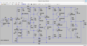
Now to the VAS.
The problem in hbt´s schematic is the to-low-impedance bias network, which is bad for THD, the ips doesn´t like that. 2,7k to the rails is way to low.
From 10k upwards is acceptable, which I used in the zdiode vas.
The original schematic used 39k.
I not need post another schematic here.
The problem in hbt´s schematic is the to-low-impedance bias network, which is bad for THD, the ips doesn´t like that. 2,7k to the rails is way to low.
From 10k upwards is acceptable, which I used in the zdiode vas.
The original schematic used 39k.
I not need post another schematic here.
Here comes the selfbiased VAS.
The base current from the upper transistor flows through the 5,6 MEG resistors back into the base of the lower transistor. No more resistors to the rails.
That results in minimal loading of the ips, lowest distortion.
Still needs the coupling caps.
The same can be done with zdiodes.


The base current from the upper transistor flows through the 5,6 MEG resistors back into the base of the lower transistor. No more resistors to the rails.
That results in minimal loading of the ips, lowest distortion.
Still needs the coupling caps.
The same can be done with zdiodes.
That hole thingy is broken by design.
There is no point in further discussions from my side.
Because
For a maximum linearity it is essential that each stage operating point is optimally biased.
i.e. in the middle of its current swing given by the circuit.
This golden rule is grossly violated making it a poor design.
My 2 cents
There is no point in further discussions from my side.
Because
For a maximum linearity it is essential that each stage operating point is optimally biased.
i.e. in the middle of its current swing given by the circuit.
This golden rule is grossly violated making it a poor design.
My 2 cents
you should read your own postingsI not need post another schematic here.
hbt insisted on keeping that vas and the inverting structure.That hole thingy is broken by design.
Beside that, how about something constructive?
hahaha...you should read your own postings
Why not?Beside that, how about something constructive?
Stop riding a dead horse!
That was the last schematic in this thread from me anyway, as I said repeatedly, I have no intention to ever buid it.Stop riding a dead horse!


- Home
- Amplifiers
- Solid State
- high performance 25W PowerAmp