I think it is pretty close, building it on a breadboard, might be a good start, to get bias verified and stable. You can use resistors from gate to source connections temporary in place of the mosfets until you measure the proper Vgs bias before inserting the mosfets, and be sure to use a bulb tester before power transformer. ") .
.
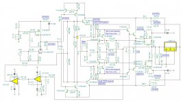
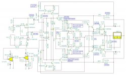
BTW I found an old thread I made awhile ago regarding this circuit HERE.. This was before I used the diamond buffer with CCS and mirror to bias input.
Also, I made an amp using HEC with Darlington bipolar, like the original concept. Example of a construction HERE. And HERE is the thread for that fabrication, if you want to call it that, ha!

 . I do recall that amp sounded surprisingly good and detailed.
. BTW I found an old thread I made awhile ago regarding this circuit HERE.. This was before I used the diamond buffer with CCS and mirror to bias input.
Also, I made an amp using HEC with Darlington bipolar, like the original concept. Example of a construction HERE. And HERE is the thread for that fabrication, if you want to call it that, ha!
. I do recall that amp sounded surprisingly good and detailed.
Last edited:
Hi
If you find that DC bias in the output mosfets increases with frequency of input signal without any load attached, try placing a cap across R14 for AC coupling between the drivers like in typical similar bipolar circuit. I used class A bias push pull drivers for each gate drive to address this problem but then, you start adding more components.......and then more....... until you end up with what I got going .....and that is how it happens. Ha ha
If you find that DC bias in the output mosfets increases with frequency of input signal without any load attached, try placing a cap across R14 for AC coupling between the drivers like in typical similar bipolar circuit. I used class A bias push pull drivers for each gate drive to address this problem but then, you start adding more components.......and then more....... until you end up with what I got going
.....and that is how it happens. Ha ha Hi,
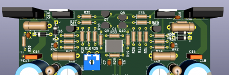
I have tested prototype. Everything looks very good. But I am not sure about one thing. For temp compensation should be both driver transistors T8 and T9 mounted on main heatsink or just one transistor?
Cordell writes in his book: "Transistor T8 is mounted on the heat sink to provide thermal feedback. Thus, about half of the total bias spread is compensated by the temperature of the heat sink. T8 is preferably a fast TO-92 transistor embedded in a hole in the heat sink."
Thank you.
Mounting both bi-polars will over compensate due to lower Gm of mosfets at bias current. I compensated for this issue by using the drain pin of mosfets to contact those transistors further from the device, in the photo in post 11, but I used SOT-323.  This is an issue that kind of depends on the fabrication, where to place the device, thermal coupling, sort of trial and error as to what arrangement tracks bias the best. I will say that mosfets are far more forgiving than bi-polars when it comes to bias adjustments. In my experience, as with the original HEC circuit if the output devices are Darlington pairs, then both transistors have to be mounted to the outputs. Much less wiggle room. Also, if you measure the output with scope ch2, and measure the emitter of T4 with ch1, invert ch2 and on the same scale, sum the two together to see the difference between the gate drive and output, or the error signal.
This is an issue that kind of depends on the fabrication, where to place the device, thermal coupling, sort of trial and error as to what arrangement tracks bias the best. I will say that mosfets are far more forgiving than bi-polars when it comes to bias adjustments. In my experience, as with the original HEC circuit if the output devices are Darlington pairs, then both transistors have to be mounted to the outputs. Much less wiggle room. Also, if you measure the output with scope ch2, and measure the emitter of T4 with ch1, invert ch2 and on the same scale, sum the two together to see the difference between the gate drive and output, or the error signal.
Last edited:
Hi.
Yeah, it is a good idea to clamp the input from the VAS to prevent any reverse bias of the drivers and improve clipping behavior. It is OK to have some fluctuation in the bias as long as it is within a reasonable range. It is another minor advantage of using mosfet outputs. . In my application, the initial cold bias starts around 60mA, but actually drops with increase in temperature to about 15 to 20mA at very high temperature. In a way the increase in Gm with temperature for mosfets kind of works in your favor.
Yeah, it is a good idea to clamp the input from the VAS to prevent any reverse bias of the drivers and improve clipping behavior. It is OK to have some fluctuation in the bias as long as it is within a reasonable range. It is another minor advantage of using mosfet outputs.
. In my application, the initial cold bias starts around 60mA, but actually drops with increase in temperature to about 15 to 20mA at very high temperature. In a way the increase in Gm with temperature for mosfets kind of works in your favor.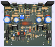
- Status
- This old topic is closed. If you want to reopen this topic, contact a moderator using the "Report Post" button.
- Home
- Amplifiers
- Solid State
- Hybrid Mu Follower Poweramp with Error Correction