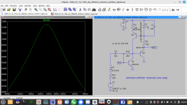
Well spotted, that's what you get for rushing@Mooly It looks like your graph is showing the sum of the outputs of the voltage driven and current driven circuits. Why have the Vout's shorted like that?
 As far as the sim goes its a valid state. Ooops!
On page 26 I count 3 x 1000uF and 2 x 4700 uF capacitors for a phono preamp ! On page 18 I count 1 x 4700 uF for the input and 1000 uF to clamp the Common Base, what kind of madness? I would not want to use any electrolytic capacitors in an audio circuit.See (this pdf), for example pages number 18 and 26.
But yes the circuit of page 18 is very like the Common Base I'm looking at but R3 and R4 at 100R each are far too low. Either they don't allow Q1 to turn on or they draw too much current.
Interesting publication.
Nope the lower the input resistance the higher is the Q A common Emitter does not boost the Q.The common base circuit has low input impedance, hence it is loading the LC circuit, lowering the Q. To have higher Q a tap should be used. In this application (at low frequency) input capacitance is not an issue, so a common emitter circuit can also be used.
Well spotted, that's what you get for rushing
Yes it is a valid state having two separate circuits input to the same graph. I have done it to compare Q of my circuit with the Common Base transistor and without it. For much the same Q the without circuit has a series resistance of 1R1 whereas the with circuit has a series resistor of 100R !!! I am plotting OP1 and OP2 on the Bode plot.
Hi Rich,
I agree that common emitter doesn't boost the Q. But common base doesn't "boost" Q either. To ensure good Q, the emitter input impedance has to be very low; in fact negative input resistance would raise the Q. The classic Q multiplier of old!
I'm betting that's what you were alluding to. Of course if negative resistance becomes larger than positive load resistance, it oscillates.
Enjoy! Best regards.
I agree that common emitter doesn't boost the Q. But common base doesn't "boost" Q either. To ensure good Q, the emitter input impedance has to be very low.
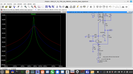
Maybe we understand boost differently. Have a look at the circuits in my post just before yours. I am comparing two circuits the first has series resistor of 1.1 Ohms R1 and the second (with the Common Base) has a series resistor of 100 Ohms R4 and the Q of both circuits is the same. So the Common Base is boosting the Q massively. If I put a 100 Ohm resistor in the other circuit it would be flat.
What I can't do is compensate for the inductor resistance (not shown) and that's where the need arises for negative resistance.
I agree that the risk is oscillation but lets say the inductor resistance is 5 Ohms and I can introduce a negative resistance of 4 Ohms then for calculation the series resistor is 1 Ohm the circuit would have very high Q and not oscillate.
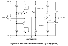
"Current feedback" amplifiers use common base transistors directly at one of the inputs. Here's a simplified schematic of an op-amp where it's easy to see that this is so (when it's in inverting configuration, with the + input grounded). You should be able to find some DIY designs like this on the forums here.That's a very specific application then, following another transistor. I'm thinking about front end applications using Common Base at audio frequencies.
Can you put up a typical circuit diagram showing Common Base front end?
In my application above the Common Base shows amazing gain but is helped by the Q of the resonant circuit.
Attachments
Common base mc pre has been used for decades.
https://leachlegacy.ece.gatech.edu/headamp/
https://leachlegacy.ece.gatech.edu/headamp/
Yes thanks @adason that's very interesting - the complimentary common base circuit etc.Common base mc pre has been used for decades.
https://leachlegacy.ece.gatech.edu/headamp/
Which transistor is in Common Base configuration please? For me its hard to see what's happening in these types of multi transistor circuits."Current feedback" amplifiers use common base transistors directly at one of the inputs. Here's a simplified schematic of an op-amp where it's easy to see that this is so (when it's in inverting configuration, with the + input grounded). You should be able to find some DIY designs like this on the forums here.
In my original circuit #1 its R1 and R2 were used to set a bias value, alternatively the Base could have been biased rather than connected to 0V. Simulating in LTspice showed that bias was critical for best performance.Hi Rich,
I agree that common emitter doesn't boost the Q. But common base doesn't "boost" Q either. To ensure good Q, the emitter input impedance has to be very low; in fact negative input resistance would raise the Q. The classic Q multiplier of old!
I'm betting that's what you were alluding to. Of course if negative resistance becomes larger than positive load resistance, it oscillates.
Enjoy! Best regards.
The following circa 1960's circuit showing the front end of an Eddystone EC10 Communications Receiver clearly uses Common Base for the front end transistor TR1.
Cunningly the original designer has got around two problems as follows:-
Firstly, the Q resonance of L3, the designer uses a tapping on L3 resonant secondary (with few turns) to feed into the Emitter of TR1 thus not loading the Q resonance of L3.
Secondly the designer uses the varying DC Automatic Gain Control (AGC) which can be manually adjustable to reach the Common Base bias "sweet spot"
C18 at 100n makes TR1 Common Base, R1, R2 and the AGC input set DC bias, TR1 Collector output is developed across L8 primary, the TR1 Emitter input comes from L3 via 1n5 C17 across the 470R resistor R3.
Secondly the designer uses the varying DC Automatic Gain Control (AGC) which can be manually adjustable to reach the Common Base bias "sweet spot"
Here is the "Magical Common Base configuration" and here also is the weakness of the Common Base configuration - the need to fine tune the Base DC bias.
I have seen several Common Base circuits where the Base bias is incorrect (not near optimal).
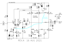
The node of Q5, Q8, Q9, U6 (& C8) is missing a resistor or current source to a lower supply rail, or there will be no current flowing through these parts at all.The circuit snippet below is part of a product that is offered for sale in the diyAudio Store: "Dreadnought". It's a field-swappable front end card for audio power amplifiers "VFET lottery" and "Ship Of Theseus".
I believe this line level pre is common-base based too.
http://tech.juaneda.com/en/projects/preamp3.html
http://tech.juaneda.com/en/projects/preamp3.html
The node of Q5, Q8, Q9, U6 (& C8) is missing a resistor or current source to a lower supply rail, or there will be no current flowing through these parts at all.
It's node "PBIAS" which was drawn with Connect-By-Name to avoid clutter.
PBIAS is 1.2V below the top supply, NBIAS is 1.2V above the bottom supply, and each of them has its own 2.2 microfarad bypass capacitor.
_
Attachments
Q1 and Q2. Imagine it's configured as an inverting amplifier, then their bases are held at a constant voltage (because the op-amp's non-inverting input pin is grounded), and their emitters are used as inputs (via the o-amp's inverting input pin).Which transistor is in Common Base configuration please? For me its hard to see what's happening in these types of multi transistor circuits.
- Home
- Amplifiers
- Solid State
- Magical Common Base configuration, why so little used?