For realizing various projects like line stage, RIAA stage, active crossover networks etc.) so as evaluation I am looking for PCB's like those under
https://www.ebay.com/itm/255197072218
https://www.ebay.de/itm/202604951103
https://www.ebay.de/itm/255197072218
and
https://www.diyaudio.com/community/threads/vacuum-tube-prototyping-pcbs-of-my-own-design.387959/
but with a single large hole appropriate for tube sockets usual used for chassis mounting (for lower thermal stress on PCB).
The image of PCB from post #2 show this - unfortunately only realized for the power tube and not for the tube for small signal application
Thanks for any advice to suppliers for such prototyping evaluation boards.
P.S.: I will use this as an alternative to the no longer available PCB from the last image in the attachment - go to
https://glass-ware.stores.turbify.net/nostmfbcr.html
Attachments
-
 tube experimenting PCB-II.jpg76.5 KB · Views: 95
 -
 tube experimenting PCB-III.jpg40.8 KB · Views: 78
 -
 tube PCB-III.jpg299.8 KB · Views: 79
 -
 tube PCB-II.jpg301.6 KB · Views: 81
 -
 tube PCB-I.jpg309.1 KB · Views: 89
 -
 tube experimenting PCB-I.jpg81.8 KB · Views: 87
 -
 PCB 180x110.jpg369.8 KB · Views: 88
 -
 PCB 250x165.jpg578.9 KB · Views: 93
 -
 noval-stereo-mfb-crossover-15.jpg87.4 KB · Views: 90
Last edited:


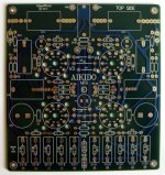
After being disappointed with turnkey solutions from eBay/Aliexpress I have designed and now use my own 250x165mm, 2.0mm thick prototyping boards, with universal pads for tube sockets, power planes on the edges of the board. I cut them into smaller pieces when necessary. Hole pitch is more convenient 5.0mm rather then 2.54mm.
Attachments


That.
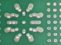
2.54mm "Veroboard" pitch is fine and perfect for SS projects, specially because you can mount DIP ICs on it, but for tube projects not necessary, at all, we use larger not so tightly spaced components.
I also made my own, in far easier to use 5.04 mm (0.2") pitch, instead of standard 0.1"
Just in case, placed a standard 14 pin 0.1" pitch DIP IC socket here and there to make it "general purpose"
Also added a row of potentiometer pinout spaced pads along one edge so long narrow boards are perfect for Guitar Preamps.
Joys of custom DIYing 😄
Was inspired by a clever British 80's Verobiard competitor, called "the Blob"
Tracks were larger as mentioned above with s few IC footprints and not drilled 😲
They were single face, used with copper tracks on top, and parts tack soldered there.
A precursor of SMT boards, go figure.
An advantage was that insulating board was undrilled, so you could simply glue them in place, or use double sided tape for mounting.
Great for quick and dirty projects.
That^I also made my own, in far easier to use 5.04 mm (0.2") pitch, instead of standard 0.1"
I use off-the-shelf boards with drilled holes, and just mount the sockets like I would do with a chassis.