I'm looking for the best, simple, way to do this on the bench without more than
a function generator (my HP goes to 11 MHz) and a scope. Our scope has a
readout of the signal amplitude and is 200 MHz. This amp is a prototype so soldering
minor changes is not a problem.
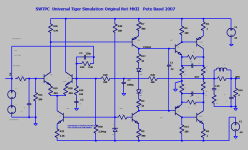
I used LTSpice to draw what I'm planning to do on the bench to measure the loop gain
of the original Universal Tiger (UT) amp. This is NOT the way to do it in simulation but
of course it will run. The best way in simulation is to use a Tian probe as explained in
these videos by one of our members:
https://www.diyaudio.com/community/...al-tiger-inconsistencies.365751/#post-7737499
Let me say that I understand that this method introduces errors but from what I
see/understand I don't think that they are significant and I welcome comments to
improve it or use another method.
The main feedback path is broken at the output and the SPICE ideal signal source drives
it. The obvious errors are that the loading on the output by the feedback network
is removed (more parts could be added to emulate it) but since the load is 4-8 ohms I
believe that the error is insignificant. The other error is that the source impedance of
the amp output is not accounted for. Now amps like this are (should be) high damping
factor and therefore the output impedance is low in the audio band. The zobel is in
parallel and should keep the impedance low at high frequencies. The circuit needs a
stable DC output and therefore a feedback network matching the pos input resistance
to ground is added with two resistors (R29, R28) and a large cap to ground to shunt
the signal. This introduces error below 1 KHz but that is not where the analysis takes
place. There was significant DC offset at the output, as is seen in real hardware, and
a very large resistor, R30, was added to trim the offset. This is not how to do it in real
hardware but with an ideal power supply in sim it works fine.
The output to measure is the point where the loop is broken with the OUT label, not
the SPK labeled net. Plotting frequency response in LTSpice is OUT/Vin from the source
which is what we want. Anyway, here's the diagram:

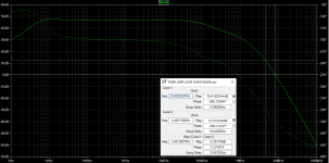
Ran it to see if the results are reasonable and what to expect on the bench:
It shows an unstable amp, but perhaps I'm missing something, we do know that these
amps certainly do oscillate in real hardware.
Odd that LTSpice does not make the two cursors different colors in the plot.
==== PHASE MARGIN
Cursor 1, furthest to the right, is at the 0dB gain point (the horizontal cursor is at 0dB)
where we should look for phase margin on the phase plot (the vertical cursor). Note
that we are driving the negative input and therefore, in the passband, we see -180 deg
as would be expected on the inverting input. The point where there is zero phase margin
is another -180 for a total of -360 bringing the signal back in phase to cause oscillation.
The amount less than -360 is the phase margin.
Note that for cursor 1 the phase is greater than -360 at about -390 and according to
this there is about -30 deg of phase margin - there is none. Keep in mind that this is
device and model dependent so real hardware could be better or worse.
Or is this not a valid method?
==== GAIN MARGIN
Cursor 2, on the left, is where the phase reaches -360 deg (vertical) and the gain
margin is how much less than 0dB the gain curve shows. The gain is actually greater
than 0dB and therefore there's negative gain margin with it showing 12.47 dB of gain
(horizontal) - it should be negative in order to have gain margin.
It should have been obvious that the stability of this amp is highly dependent on the
process variation of the semiconductors which is demonstrated by the fact that I have
one amp that readily oscillates and another of the same revision that does not.

a function generator (my HP goes to 11 MHz) and a scope. Our scope has a
readout of the signal amplitude and is 200 MHz. This amp is a prototype so soldering
minor changes is not a problem.
I used LTSpice to draw what I'm planning to do on the bench to measure the loop gain
of the original Universal Tiger (UT) amp. This is NOT the way to do it in simulation but
of course it will run. The best way in simulation is to use a Tian probe as explained in
these videos by one of our members:
https://www.diyaudio.com/community/...al-tiger-inconsistencies.365751/#post-7737499
Let me say that I understand that this method introduces errors but from what I
see/understand I don't think that they are significant and I welcome comments to
improve it or use another method.
The main feedback path is broken at the output and the SPICE ideal signal source drives
it. The obvious errors are that the loading on the output by the feedback network
is removed (more parts could be added to emulate it) but since the load is 4-8 ohms I
believe that the error is insignificant. The other error is that the source impedance of
the amp output is not accounted for. Now amps like this are (should be) high damping
factor and therefore the output impedance is low in the audio band. The zobel is in
parallel and should keep the impedance low at high frequencies. The circuit needs a
stable DC output and therefore a feedback network matching the pos input resistance
to ground is added with two resistors (R29, R28) and a large cap to ground to shunt
the signal. This introduces error below 1 KHz but that is not where the analysis takes
place. There was significant DC offset at the output, as is seen in real hardware, and
a very large resistor, R30, was added to trim the offset. This is not how to do it in real
hardware but with an ideal power supply in sim it works fine.
The output to measure is the point where the loop is broken with the OUT label, not
the SPK labeled net. Plotting frequency response in LTSpice is OUT/Vin from the source
which is what we want. Anyway, here's the diagram:

Ran it to see if the results are reasonable and what to expect on the bench:
It shows an unstable amp, but perhaps I'm missing something, we do know that these
amps certainly do oscillate in real hardware.
Odd that LTSpice does not make the two cursors different colors in the plot.
==== PHASE MARGIN
Cursor 1, furthest to the right, is at the 0dB gain point (the horizontal cursor is at 0dB)
where we should look for phase margin on the phase plot (the vertical cursor). Note
that we are driving the negative input and therefore, in the passband, we see -180 deg
as would be expected on the inverting input. The point where there is zero phase margin
is another -180 for a total of -360 bringing the signal back in phase to cause oscillation.
The amount less than -360 is the phase margin.
Note that for cursor 1 the phase is greater than -360 at about -390 and according to
this there is about -30 deg of phase margin - there is none. Keep in mind that this is
device and model dependent so real hardware could be better or worse.
Or is this not a valid method?
==== GAIN MARGIN
Cursor 2, on the left, is where the phase reaches -360 deg (vertical) and the gain
margin is how much less than 0dB the gain curve shows. The gain is actually greater
than 0dB and therefore there's negative gain margin with it showing 12.47 dB of gain
(horizontal) - it should be negative in order to have gain margin.
It should have been obvious that the stability of this amp is highly dependent on the
process variation of the semiconductors which is demonstrated by the fact that I have
one amp that readily oscillates and another of the same revision that does not.

Last edited:
Long ago when I was still in the workforce we used 'Bode boxes' to inject signals into a closed feedback loop. I offer this just for info and do not claim this is best technique now.
https://www.venableinstruments.com/accessories/frequency-response-analyzers/bode-boxes
https://www.venableinstruments.com/accessories/frequency-response-analyzers/bode-boxes
Just remembered/noticed that the outputs are MUCH faster than the original MJ4502/802 outputs
this of course could throw off the simulation.
I know that the SPICE models for the original, slow outputs were defective from Onsemi, does anyone
know of good models or similar devices?
Could also use 40409/40410 models.
this of course could throw off the simulation.
I know that the SPICE models for the original, slow outputs were defective from Onsemi, does anyone
know of good models or similar devices?
Could also use 40409/40410 models.
You can plot the gain/phase of the ratio V(out)/V(R18). That is the gain within the loop minus the differential gain of the phase splitter, which is close to 1.
Hello Pete,
Interesting topic.
Maybe a stupid question, but how do you deal with the 47 dB OLG in case the amp-on-the bench is fed an input signal of 1 Volt? I suppose you use a 47 dB padding down network?
@Bill_P: is padding down level what these Bode boxes, apart from not loading and isolating the DUT, do?
Interesting topic.
Maybe a stupid question, but how do you deal with the 47 dB OLG in case the amp-on-the bench is fed an input signal of 1 Volt? I suppose you use a 47 dB padding down network?
@Bill_P: is padding down level what these Bode boxes, apart from not loading and isolating the DUT, do?
Here is what I remember about applying Bode boxes from more than 20 years ago. We had three boxes to cover the range of 10's of Hz to 100kHz or so. The new boxes on the web today seem to have a wider frequency range. The old boxes contained a ferrite pot core transformer. I don't recall what the turns ratio was. There may have been a coupling capacitor on the primary - I can't recall for certain.
The idea was to break the feedback loop at a spot where the driving impedance was much higher than the input impedance. Often the point where the feedback loop connected to the output would meet this requirement. The Bode box secondary was connected at this point which provided DC continuity for the loop as well as measurement points for gain and phase.
We used a Hewlett Packard network analyzer to drive the Bode box primary with a tracking generator and then put probes on both sides of the Bode box secondary. The network analyzer would measure amplitude and phase for both probe points and display the ratio of the two in a gain-phase plot.
This is what we did in ancient times. There may be better methods now. We had no inkling about Tian probes and such back then.
I made a Rogowski coil with some transformer wire and a small ferrite toroid. That worked pretty well for injecting a signal into the feedback loop. I then used an HP 3575 network analyzer to plot the loop gain.
Another trick is to rig your amp as an inverting amp with a gain of -1 V/V. Then measure the error voltage, i.e., the voltage from IN+ to IN-. It'll be the inverse of the loop gain, so you have to invert the curve (in dB) in your head.
Tom
Another trick is to rig your amp as an inverting amp with a gain of -1 V/V. Then measure the error voltage, i.e., the voltage from IN+ to IN-. It'll be the inverse of the loop gain, so you have to invert the curve (in dB) in your head.
Tom
@Boden I've not yet done the measurement but why not feed it .01V of signal or less? Or if the output is at large signal, yes pad it down.Hello Pete,
Interesting topic.
Maybe a stupid question, but how do you deal with the 47 dB OLG in case the amp-on-the bench is fed an input signal of 1 Volt? I suppose you use a 47 dB padding down network?
@Bill_P: is padding down level what these Bode boxes, apart from not loading and isolating the DUT, do?
In my last post I got the impedances backwards. The driving impedance should be much lower than the input impedance.
The HP analyzer I used was the 4194A.
Regarding signal level, maintaining a high signal to noise ratio while avoiding overload is desired. To check for overload run a gain-phase plot and then repeat with 6dB less input signal. If the plots do not overlay there is compression due to overload. Run the input signal amplitude up and down to find the overload point and back off 6 to 10 dB for the final plot.
ah, finally learned the name of that test component, Bode box (note to myself: remember this)!...we used 'Bode boxes' to inject signals into a closed feedback loop...
Back some 20+ years ago we used a HP 3577A and a homebrew bode box made up of a ferrite toroid ca 5-6 cm in diameter, the primary had relatively many turns, now I don't remember much at all the winding design of that bode toroid but somehow recall it may have had two secondaries.., one for the signal injection into the feedback loop of whatever is to be measured, the other secondary was connected to the network analyzer, and again not remembering very well but was it so that before measuring, the box was swept through the frequency range set to be measured so as to have a reference towards which the measured feedback loop was compared against to get the gain and phase(?), or maybe I'm mixing some things up because I also used the analyzer to characterize passive components, there one had to first run a sweep of the test jig without the dut component in place.
The injection signal should be pretty small to verify the small signal characteristics and avoiding large signal behavior creeping in muddling the result.
Anyone know of any DIY bode box to be used with network analyzer please shout out as I would like to make one for me.
Attachments
I tried this per the schematic in the first post but used a 10uF mylar cap for C7. It oscillates at 45 KHz, square wave 55Vpp.
Changed cap to a .1 uF oscillates at 67 KHz. Removed C7 and it oscillates at 86 KHz.
Strange, needs better power supply decoupling?
Changed cap to a .1 uF oscillates at 67 KHz. Removed C7 and it oscillates at 86 KHz.
Strange, needs better power supply decoupling?
Let me mention again that this is the amp that didn't oscillate at all.
From the last post this amp oscillates simply by raising the feedback resistor to 20K total.
I changed them to two 2.2K and yesterday it didn't oscillate with the cap out, today it does.
Changed to one 2.2K and it doesn't oscillate but along the way here I added a pair of
100uF from the rails to ground. Now, with one 2.2K it bursts into oscillation when I remove
the fuse which removes the 8R load and .1uF to ground. Oscillation is at 520KHz but it I
remove the 100uF bypass caps it becomes stable again.
I didn't use resistors in the supply rails to decouple the front end but this is not good.
The other amp oscillates around 3 MHz.
Definitely more than 20 years ago. Sometime before that I recall attending an HP seminar on measuring power supply (and or other control loop) gain and phase margin using a signal injection transformer and a VNA. It was a big thing at the time because milspec power supplies had to meet a new proof of stability requirement. Still have the printed app note around here somewhere....applying Bode boxes from more than 20 years ago.
Here are some examples of injection transformers. It's necessary to observe the voltage isolation ratings.
https://www.newtons4th.com/products...zers/frequency-response-analyzer-accessories/
https://www.newtons4th.com/products...zers/frequency-response-analyzer-accessories/
- Home
- Amplifiers
- Solid State
- Measuring Loop Gain on the Bench - Best Way?