1. You have independent current sources I1 and I2 instead of mirroring out the current through Q7 and Q6.
When I1 and I2 were replaced with cascaded current sources, the output was inverted.
I noticed that I1 and I2 are cascade currents of the drive current, but I never thought that the output would be inverted.
Even if the area is x1, the gain is reduced, but the polarity is reversed.
I think I finally understand it.
Driving Q1 and Q2 (with your numbering) has essentially no effect, as it affects the currents through Q3 and Q4 equally and contributes essentially nothing to the output current.
The current mirrors simply mirror the drive currents and inject them at the normal locations: the bases of the output transistors. Hence the sign inversion. As Elvee's mirrors have a 1:4 ratio, they increase the magnitude of the loop gain by a factor of four.
OK, I see how it works: each half drives the opposite side.
However, if we make a fair comparison between the two drive options, the alternative drive shows a definite superiority.
First, the regular method:

The THD is 0.67%
The alternative is simpler, and offers 0.031% THD, 1/20th:

The input impedance is much lower, ~10K but still acceptable.
The improvements do not come from the core linearity: it is approximately equivalent. The current gain is somewhat higher, but it is insufficient to explain the good performance, meaning an unidentified effect is responsible; the impedance seen by the FB divider looks like a plausible candidate
However, if we make a fair comparison between the two drive options, the alternative drive shows a definite superiority.
First, the regular method:
The THD is 0.67%
The alternative is simpler, and offers 0.031% THD, 1/20th:
The input impedance is much lower, ~10K but still acceptable.
The improvements do not come from the core linearity: it is approximately equivalent. The current gain is somewhat higher, but it is insufficient to explain the good performance, meaning an unidentified effect is responsible; the impedance seen by the FB divider looks like a plausible candidate
I think that the 20 times difference in distortion factor can be explained by the difference in loop gain.
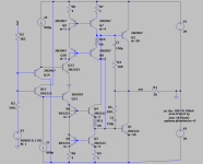
First is the drive circuit. The original circuit has 0.2mA flowing through Q13 and Q14. Therefore gm = 7.8mS and the composite gm is 15.6mS. However, due to self-feedback due to R2//R3 = 375Ω in the feedback network, it degenerates to 2.28mS.
On the other hand, the alternative is to drive the emitters directly with a voltage signal source, resulting in no degeneracy and still 15.6mS. (The emitters of #52's inverting amplifier circuit is also directly grounded.)
There is already a 6.8x difference here.
And in the core part, in the original circuit the drive current drives the bases of Q1, Q2 directly, whereas in the alternative, the drive current goes through a 1:4 current ratio mirror of Q9, Q7 and Q5, Q3, thus being inverted. drives the bases of Q1 and Q2. Therefore, there is a gain difference of about 27 times in total.
Last edited:
I agree: the improvement stems from the higher gain and the elimination of the Thevenin equivalent of the FB network.
It remains an improvement though, since there are practically no penalties for adopting it, meaning it is almost free, except for the input impedance reduction
It remains an improvement though, since there are practically no penalties for adopting it, meaning it is almost free, except for the input impedance reduction
I am trying to apply the circuit to my instrument amplifier.
I have adopted the "irregular" driving scheme, and begun to add some degeneration for use with discrete components.
At the moment, the stability is not addressed properly, which means it breaks into oscillations after ~300µs, but it highlights another issue: a propensity to latch-up. When overdriven, the inverting path is not dominant anymore, and latch-up occurs:

Such a behaviour is not acceptable, even in a stable circuit, and has to be rooted out.
Unfortunately, I do not see a simple, elegant way to do it without ruining the performance. Any ideas?
I have adopted the "irregular" driving scheme, and begun to add some degeneration for use with discrete components.
At the moment, the stability is not addressed properly, which means it breaks into oscillations after ~300µs, but it highlights another issue: a propensity to latch-up. When overdriven, the inverting path is not dominant anymore, and latch-up occurs:
Such a behaviour is not acceptable, even in a stable circuit, and has to be rooted out.
Unfortunately, I do not see a simple, elegant way to do it without ruining the performance. Any ideas?
Attachments
Common emitter stages with emitter resistors can reverse polarity when the transistors go in deep saturation; a common emitter stage is supposed to invert, but a forward-biased base-collector diode doesn't. Does Q7 or Q3 go far enough in saturation for the polarity to reverse?
If so, you have to limit the currents through them, or put a voltage clamping device somewhere.
If not, can you plot a schematic with all node voltages annotated on it?
If so, you have to limit the currents through them, or put a voltage clamping device somewhere.
If not, can you plot a schematic with all node voltages annotated on it?
Well that's interesting. LV's simulation latches up hard due to phase inversion when the current in R9 saturates Q3 leaving only an inverted path through Q4. I got it to work by reducing the mirror resistors to almost nothing, so that Q3 (and Q7) remain the dominant signal path.
I think the key to this topology is that the base current of the OPs is reflected to the other OP, so that when one fall off, it boosts the other, much the same as EF cross-coupling. So, a MOS version would not benefit as much from this topology as the gates remain Hi-Z as the device conducts.
But with LV's drive points, the collector current in the cross coupler cascode transistors is inverted.
Attachments
Last edited:
Yes they do, as Steve also noticed.Does Q7 or Q3 go far enough in saturation for the polarity to reverse?
Limiting the available current is an option, and it is the first I tried:
Resistors are simple and effective, but they are also crude and brutal: they introduce unwanted poles, and for an amplifier that is supposed to handle 1MHz transparently, it's a no-no.
Is there a subtler way of limiting the current? Certainly, but how complicated is it going to be?
Similarly, I don't see a simple and accurate method capable of clamping the voltage: the excursions are quite small, and I don't want to introduce non-linearities before the actual clamping action.
When all of that is solved, another problem needs to be tackled: the compensation. The method I have (provisionally) used is certainly suboptimal, but where else to apply it?
Since the circuit will oscillate as it is, I changed C1 and C2 to 330pF and set R4 and R5 to 0Ω. (from lag-lead compensation to lag compensation)

This stopped the oscillation (5V input - dotted line), but when the input is set to 7V and the output is clipped, it is saturated and inverted at the same time, and after that it becomes a square wave state (solid line).

In order to prevent overdriving when the output is clipped, constant current diodes are placed in the collector of Q12 and Q13 so that it is in the linear region (although not linear at all ) as low resistance during normal operation and in the saturated region (constant current) during output saturation. When inserted, it became a normal clip waveform.
(actually CRD are 2SK117 with Idss=13mA models)


I'm not sure if this is the simple and elegant way Elvee calls it.
This stopped the oscillation (5V input - dotted line), but when the input is set to 7V and the output is clipped, it is saturated and inverted at the same time, and after that it becomes a square wave state (solid line).
In order to prevent overdriving when the output is clipped, constant current diodes are placed in the collector of Q12 and Q13 so that it is in the linear region (although not linear at all
) as low resistance during normal operation and in the saturated region (constant current) during output saturation. When inserted, it became a normal clip waveform.(actually CRD are 2SK117 with Idss=13mA models)
I'm not sure if this is the simple and elegant way Elvee calls it.
Last edited:
Clamping the voltage will not prevent Q12 and Q13 from burning out when the amplifier is driven into clipping, so I think limiting the current is the only practical approach. Mason_f8's solution is a nice one. An inelegant alternative could be Elvee's resistors shunted with small capacitors (no larger than needed to keep the effect on stability small).
- Home
- Amplifiers
- Solid State
- Monticelli: Ultra-Efficient, Ultra Low Distortion