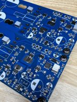
Mooly slim SMD version now built (minus MOSFETS as yet).
Wow, that looks really cool in smd form.
Close up pictures can be very very revealing... those look pretty good to me. Stand back a few inches and it will near perfectI've managed to solder them in place but they're not ideal by any means.
") No chance of any dies either looking at those.
No chance of any dies either looking at those.Nice work


I've finally lashed a power supply together. The only transformer I had in my spares box has two secondary windings at 25V/1A so provides an unregulated +/-38Vdc. So for now I'm only going to be able to do the dc measurements. On initial switch-on:
- the output voltage was +5.6V instead of an expected 0V +/- a few mV
- the output from the op-amp was -0.1V instead of expected -5.6V (or thereabouts)
- the -ve supply to the op-amp was only -7V as opposed to the expected -12V
To verify that the dc servo was the problem, it was isolated from the rest of the circuit and bias for T1 provided by a potentiometer in place of the op-amp output. Adjusting it to between -5 and -6V enabled the amp's Vout to achieve its nominal 0V . This confirmed the dc servo was the problem. Replacing the 0.1uF film cap with a ceramic one of the same value from my spares box fixed the problem and measured Vout (at junction of R19, R20) for the amp was now +0.84mV.
The highest dissipation transistors for the circuit are T3 and T5. At +/-45V, this is expected to be around 230-240mW. With the 3+/_38Vbeing applied, this will be about 200mW. Using a finger as a temperature probe, T3 is no warmer than any of the other transistors and T5 is only slightly warmer so shouldn't give any problems once the MOSFETs are added and it gets run at higher powers. That's it for now...

Considering the KiCad footprint for the 0.1uF film capacitor I chose was the "handsolder" option for the 2220 film SMD size, there isn't much pad visible to get your soldering iron tip or solder onto. Its quite a physically large block in comparison to the pad and not at all easy to solder in place - I expect it got cooked.Very unusual to have a faulty film cap these days... nice bit of fault finding there
The ceramic chip I put back on was so much easier and had the advantage of working!
"Its quite a physically large block in comparison to the pad and not at all easy to solder in place - I expect it got cooked."
I didn't check the component fitment yet, but this makes sense, SMD film caps do not like hot iron touches for any length of time 🔥.
I didn't check the component fitment yet, but this makes sense, SMD film caps do not like hot iron touches for any length of time 🔥.
Thinking about the issues soldering the large film capacitor in place onto the existing pads for the device, I took a look at what else is available as a 0.1uF highish voltage capacitor and the use its being put to within the overall amplifier circuit. Instead of the film cap, I would be inclined to use an MLCC ceramic in an 1812 case size for all of the locations where its used. That would beConsidering the KiCad footprint for the 0.1uF film capacitor I chose was the "handsolder" option for the 2220 film SMD size, there isn't much pad visible to get your soldering iron tip or solder onto. Its quite a physically large block in comparison to the pad and not at all easy to solder in place - I expect it got cooked.
The ceramic chip I put back on was so much easier and had the advantage of working!
- C8 - integrator capacitor (the one I killed with soldering)
- C9 - part of the Zobel network
- C12, C13 - supply rail decoupling
This amp has been in queue for quite some time.... finally the build has started!
Tonights task was to complete all the surface mount soldering, mission completed.
Still undecided if single or dual die Exicon's should be used?
I switch between two speaker sets, an 8R pair and a 4R pair.
Would the ECW20P20/20N20 FET's be the better option to handle either of my speaker choices?
Aiming to keep the power supply close to +/-45V.
Attachments
Would the ECW20P20/20N20 FET's be the better option to handle either of my speaker choices?
I think a few have used the double die FET's but as I always say, it is an untested change to the original design. My B&W703's dip to 3 ohm (2.8 I believe in one review) and it has no trouble driving these with the original single die Hitachi/Renesas parts.
(The old Maplin lateral FET was specced at 100wrms into 8 ohm and 150 wrms into 4 ohm with -/+55 volt supplies and used the T03 2SJ50/K135 pair)
That's good for 100W into 8ohm. It's what I'm intending to do alsoAppreciate the feedback Mooly.
Yeah, I’ll go with the ‘as designed’ FET’s. 👍🏻
Hi Karl,Thinking about the issues soldering the large film capacitor in place onto the existing pads for the device, I took a look at what else is available as a 0.1uF highish voltage capacitor and the use its being put to within the overall amplifier circuit. Instead of the film cap, I would be inclined to use an MLCC ceramic in an 1812 case size for all of the locations where its used. That would be
The 1812 cap will easily solder onto the existing pads.
- C8 - integrator capacitor (the one I killed with soldering)
- C9 - part of the Zobel network
- C12, C13 - supply rail decoupling
Bearing in mind the susceptibility of SMD films to heat when soldering them, would there be any issues from a circuit design viewpoint to using COG ceramics in place of the original films?
On my present board layout, the 1812 case size can easily be fitted onto the 2220 case size footprint/pads that are currently there, Comparing the recommended land areas from the Kemet data sheet, KiCad has these undersized.
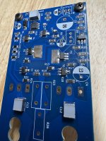
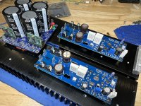
Heatsinks prepped and the boards are assembled minus output Fets, thinking about powering the boards to confirm the servo is working before mounting the Exicons. Still need to wind the inductors.
Hammond 300VA, 2 x 30V trafo and Prasi’s compact CRC board configured as CC and active rectification for the power supply.
Does the I/P Ground (J2) pad on the amp board connect to the power supply ground?
Getting close…..
Hammond 300VA, 2 x 30V trafo and Prasi’s compact CRC board configured as CC and active rectification for the power supply.
Does the I/P Ground (J2) pad on the amp board connect to the power supply ground?
Getting close…..
Attachments
Does the I/P Ground (J2) pad on the amp board connect to the power supply ground?
Have a read at this thread which I'll pick up here at post #38, but look before and after this.
https://www.diyaudio.com/community/threads/3-stage-lin-topology-nfb-tappings.101321/post-1624677
https://www.diyaudio.com/community/threads/3-stage-lin-topology-nfb-tappings.101321/post-1626642
And it's worth reading through Bonsai's excellent write-up on wiring up amplifiers https://hifisonix.com/wp-content/uploads/2019/02/Ground-Loops.pdfDoes the I/P Ground (J2) pad on the amp board connect to the power supply ground?
Getting close…..
Both boards now built (minus MOSFETs) and dc tested. As previously mentioned, the first board had a problem with the dc servo due to a cooked film capacitor. For the second board, my deliberate mistake was fitting the op-amp back-to-front. Once swapped back to the correct orientation, it worked as advertised.

I now need to rig up my heatsinks, fit the MOSFETS and start running a few checks with a dummy load. Onwards and upwards!
I now need to rig up my heatsinks, fit the MOSFETS and start running a few checks with a dummy load. Onwards and upwards!
Simultaneous builds here.😁
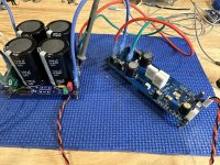
Powered up Amp#1:
Supply: +/-44V
Opamp pin4: -11V85
Opamp pin6: -4V85
R19/20 junction: 1mV
Temp. T3/T5: 38°C
The temperature was checked with thermocouple attachment for Fluke DMM touching the BJT body.
Amp#2 measured basically the same, no need to repeat.
Next up is mounting the Latfets and inductor winding….
Attachments
- Home
- Amplifiers
- Solid State
- My MOSFET amplifier designed for music