ok, so i have now made the new rear terminal assemblies and i just have to attached to the PCB's.
Im going to attempt to re create the missing phono boards in KICAD as suggested by @Goldie99 , so keep an eye out for that one.
I still have a few jobs left to do with this one yet ,so its going to take a while
Im going to attempt to re create the missing phono boards in KICAD as suggested by @Goldie99 , so keep an eye out for that one.
I still have a few jobs left to do with this one yet ,so its going to take a while
Attachments
ive made a start with the board,and i havent gone far yet, but it isnt easy to get the footprints right for the components, so if there is anyone out there with experience of using Kicad, it would be appreciated with a bit of guidance

thanks
thanks
Seems ok so far - you seem to be using a more recent version of Kicad than I do (I'm still on 6.0), but the fundamentals will all be the same.
The key point is - Kicad needs to 'fully understand' exactly which part is which, what type of part it is electrically, how it is connected into the circuit, and what it's physical dimensions are, and how / where the pcb will connect to the rest of the world.
The first stage is the schematic that you're already working on. Once you've got the schematic finished (just for the phono stage board), you can use the 'Fill in Schematic Reference Designators' button to either add reference numbers to all parts automatically, or enter them manually - it'll tell you it you've missed any. If you want the part designations to match the NAD schematics you'll need to enter them manually, as you seem to be doing. The designations will appear on the final pcb silkscreen layer (if you choose to use one), and are used when you come to lay out the pcb itself.
With the schematic finished, and all parts having reference designations, you can use the 'Perform Electrical Rules Check' button to check that everything is connected properly, e.g., every resistor has 2 connections, every transistor has 3 connections, etc. etc. If & when it finds any errors it'll display a full itemised list of every error & warning - they all need to be addressed / corrected before continuing beyond the schematic. You'll have some errors certainly, e.g., remember, when you have a power supply say, it needs to connect to the circuit (pcb) somewhere, so you need to add a terminal for that, a terminal for any ground connection, terminals for signal inputs / outputs, etc. - basically all the 'connections' going into / out of the finished pcb. You can just use the ERC button multiple times as you go through making the corrections.
Once the ERC is correct, you'll need to assign the component values, and footprints (e.g., the part physical dimensions), for every part - that's what the next button is for, the 'Footprint Assignment Tool'. The vast majority of parts that you'll need will already be available in the selection lists in that tool - if you don't know any part dimensions, just either measure them, or better still, look them up online - Mouser lists physical dimensions for virtually everything, and/or gives links to the original part datasheets. Tip - all your resistors will probably be the same type & size, you might need 2-3 differenct cap sizes, maybe a couple of transistor types, and a few terminals, a lot will be repeated so it's far less daunting than it might seem.
The next step once that's all done is to 'open the pcb in the board editor' - it'll look a mess to start, but it's actually an extremely powerful tool, that just takes some getting used to. You've probably already seen it during the tutorials I linked to previously. Let me know when you get that far or if you get stuck, but I'm no expert by any means...
Anyway, if you work through the various steps, it should all drop into place relatively easily - it does take some getting used to, but it'll probably 'clcik' at a certain point, and this is quite a nice small pcb to start with.
I've never tried it, but I don't see why the pcb couldn't be the same shape as the originals. You define the final pcb dimensions & shape in Kicad, and the NAD shape is certainly possible in that respect. In the worst case though, you could define rectangular with edge connectors on the bottom edge (to match the NAD pcb slots).
Any Kicad experts about ?
Any Kicad experts about ?
This might not help as regards learning how to use KiCad but for a small simple board like that I would measure the size first and put those dimensions into the program and then just draw it 'freehand'. Just work from the board layout in the manual, its only a few pads and traces. I'm assuming you can do that with KiCad in the way you can with DipTrace. You don't even need silkscreen component references on it.
The autorouter in KiCad won't route the same as the original but as Goldie mentions, you would have to define the edge connectors as the points to use for the in's and out's on the board.
The autorouter in KiCad won't route the same as the original but as Goldie mentions, you would have to define the edge connectors as the points to use for the in's and out's on the board.
I've never found an autoroute option in Kicad (up to 6.0 anyway), but otherwise, that's how I'd route everything as well (it helps to have the part designations while laying it out in Kicad).
I have finished the scheme, but i must have things wrong or missing.It is showing the errors, but im not quite sure what it is sayingSeems ok so far - you seem to be using a more recent version of Kicad than I do (I'm still on 6.0), but the fundamentals will all be the same.
The key point is - Kicad needs to 'fully understand' exactly which part is which, what type of part it is electrically, how it is connected into the circuit, and what it's physical dimensions are, and how / where the pcb will connect to the rest of the world.
The first stage is the schematic that you're already working on. Once you've got the schematic finished (just for the phono stage board), you can use the 'Fill in Schematic Reference Designators' button to either add reference numbers to all parts automatically, or enter them manually - it'll tell you it you've missed any. If you want the part designations to match the NAD schematics you'll need to enter them manually, as you seem to be doing. The designations will appear on the final pcb silkscreen layer (if you choose to use one), and are used when you come to lay out the pcb itself.
With the schematic finished, and all parts having reference designations, you can use the 'Perform Electrical Rules Check' button to check that everything is connected properly, e.g., every resistor has 2 connections, every transistor has 3 connections, etc. etc. If & when it finds any errors it'll display a full itemised list of every error & warning - they all need to be addressed / corrected before continuing beyond the schematic. You'll have some errors certainly, e.g., remember, when you have a power supply say, it needs to connect to the circuit (pcb) somewhere, so you need to add a terminal for that, a terminal for any ground connection, terminals for signal inputs / outputs, etc. - basically all the 'connections' going into / out of the finished pcb. You can just use the ERC button multiple times as you go through making the corrections.
Once the ERC is correct, you'll need to assign the component values, and footprints (e.g., the part physical dimensions), for every part - that's what the next button is for, the 'Footprint Assignment Tool'. The vast majority of parts that you'll need will already be available in the selection lists in that tool - if you don't know any part dimensions, just either measure them, or better still, look them up online - Mouser lists physical dimensions for virtually everything, and/or gives links to the original part datasheets. Tip - all your resistors will probably be the same type & size, you might need 2-3 differenct cap sizes, maybe a couple of transistor types, and a few terminals, a lot will be repeated so it's far less daunting than it might seem.
The next step once that's all done is to 'open the pcb in the board editor' - it'll look a mess to start, but it's actually an extremely powerful tool, that just takes some getting used to. You've probably already seen it during the tutorials I linked to previously. Let me know when you get that far or if you get stuck, but I'm no expert by any means...
Anyway, if you work through the various steps, it should all drop into place relatively easily - it does take some getting used to, but it'll probably 'clcik' at a certain point, and this is quite a nice small pcb to start with.
If you look at the schematic carefully, the ERC tool has dropped a couple of small red arrows into it, pointing at errors - double click on any of the items in the list of errors and it should highlight the specific part of the schematic that needs fixing, so you can work through them easily.
You have something labelled R1 or RL at the signal input - Kicad thinks 'R' mean resistor so is showing it as an error (unannotated R?) - I'd change the signal input to 2 single terminals (one labelled 'signal', one 'signal ground'), the NAD pcb uses separate signal and power grounds if I recall, so they need to be separate in the schematic also.
You seem to have labelled the voltage rails and GND, but not added any terminal connections for them - just use 'add component' to add a terminal or connector wherever needed, e.g., one terminal connected on the schematic to one of the GND points is sufficient to connect ALL of the positions labelled as the GND net. The power supplies are aslo missing connectors. Note - once the connectors are all added, they will also be annotated, the same as every other part on the schematic. The annotations are useful when you get to the pcb, it helps keep track of what's where, but it's also the basis the silkscreen text on the final pcb, and is also completely editable as you'll see further on - so you can add transistor names, emitter labels, connection labels etc. etc. (later).
im having a bit of trouble at this point.
with regards to the connectors, i presume ,at this stage(or not) the connectors need to represent the final application? if so these are just flat soldered bits of board, and nothing like that is represented in the choices for any connectors.I also cannot find anything other than what i picked that resembles a standard rca connector.
Most of what is in the lists appertain to digital applications,or it appreas so.
when you say the item isnt anotated, do you mean labeled?
You need the connectors for Kicad to be able to identify what connects to what in the (3D) pcb world, e.g., you have some kind of '+ 23' label on the +ve supply rail at the moment, that's fine for labelling the schematic, but the label on it's own has no meaning for Kicad in the 3D world. It needs to have an identifiable, unique, component to position on the pcb. That's what the connector is for, even though it will never actually be used, and will possibly only ultimately be an exposed strip of pcb track (for this NAD pcb).
For single point connection I tend to use this one: it has only one connection going to it (the '1' in the symbol); 'Conn_01x01' just means it's a connector with 1 row and 1 colunn of terminals, so in other words just one terminal, 02x02 would have 4 terminals, etc.
The 'J2' is the part annotation - it's the equivalent of say R2, R5, C3 etc. on a schematic, it just identifies which connector it is. They don't exist / appear at all in the NAD schematics, so you can just let Kicad do it's thing and annotate them automatically and they'll end up as J1, J2, J3 etc.
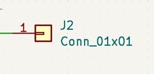
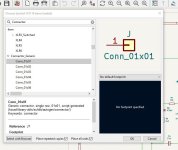
To add the connector, you just use the 'add part' button, and search for 'connector' - scroll down to whichever connector you need - note, this one has a symbol, as in the image above, but no footprint attached to it. I tend to use just a 1.0mm diameter pin footprint, unless or until I need to change or update it later on. You assign the footprint in the same way as you assign any other footprint - a selection of 1.0mm diameter pins are available in the standard list.
Just as an example, this is what 3 of them look like in the 3D viewer (further on) - using 1.0mm diam / 10mm long pins:
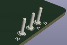
These are just one example, you'll see there are thousands of possible options in Kicad.... and it's extremely versatile, so if say something doesn't 'look' right in the 3D pcb viewer at the end, you just go back, edit whatever's necessary and effectively iterate to the final design you want. I lost count of the number of times I had to tweak something with the first pcb I put together - but that's how you learn the software, and I'm still VERY far from an expert. There is however a lot of guidance already online for Kicad, esp once you get over the initial hurdles (I had this same problem with the connectors early on...).
For single point connection I tend to use this one: it has only one connection going to it (the '1' in the symbol); 'Conn_01x01' just means it's a connector with 1 row and 1 colunn of terminals, so in other words just one terminal, 02x02 would have 4 terminals, etc.
The 'J2' is the part annotation - it's the equivalent of say R2, R5, C3 etc. on a schematic, it just identifies which connector it is. They don't exist / appear at all in the NAD schematics, so you can just let Kicad do it's thing and annotate them automatically and they'll end up as J1, J2, J3 etc.

To add the connector, you just use the 'add part' button, and search for 'connector' - scroll down to whichever connector you need - note, this one has a symbol, as in the image above, but no footprint attached to it. I tend to use just a 1.0mm diameter pin footprint, unless or until I need to change or update it later on. You assign the footprint in the same way as you assign any other footprint - a selection of 1.0mm diameter pins are available in the standard list.

Just as an example, this is what 3 of them look like in the 3D viewer (further on) - using 1.0mm diam / 10mm long pins:

These are just one example, you'll see there are thousands of possible options in Kicad.... and it's extremely versatile, so if say something doesn't 'look' right in the 3D pcb viewer at the end, you just go back, edit whatever's necessary and effectively iterate to the final design you want. I lost count of the number of times I had to tweak something with the first pcb I put together - but that's how you learn the software, and I'm still VERY far from an expert. There is however a lot of guidance already online for Kicad, esp once you get over the initial hurdles (I had this same problem with the connectors early on...).
Hi Poundy
Great to see you bringing life back to a NAD 3030. I'm sure it will be sounding fine, and be HiFi and maybe not High End 🙂
I have bden the happy owner of a NAD 3020 bought after my confirmation 🙂
Keep it original, don't change the output transistors. Newer types will have other characteristics, and you will have to at least ensure no oscillation and other ill effects.
For the phono amp, have you considered using SMD components? You can have JLCPCB mount most at very little extra cost.
If you share the KiCad files I can help you. You need to find out how the PCB outline should be, and as Goldie99 says ensure the right pin put so that it fits down in the main pcb.
As Goldie99 says you should define the connector row (pin row) that you will connect all in, out and power to, that will be the interface to the main board.
Can you also share the original phono schematics in order to check?
Go for it

- Home
- Amplifiers
- Solid State
- NAD 3030 complete rebuild


