I have used both similar shunt-regulator and simple low-noise LDO (LP5907) with clocks (NZ2520SDA). No noticeable difference in DAC/ADC noisefloor or phase noise. Maybe you should add LP5907 to your board so you could test both.
Now with added LP5907 + 1uF caps OR resistor + shunt. I may move the DC side right a little as that ground via matrix next to the oscillator is getting claustrophobic.

LP5907 is very good LDO, and for the digital circuits (including oscillators) it is more than enough.
Like most LDOs it will still need ferrites etc to cope with HF.
I've essentially finished the design - I need to double check the pins against the data sheets for the ICs etc. These can be populated by either a PL5907 with two caps or the shunt. There's also edges free of mask to make box. I've included a multi-turn borns pot for initial testing that way if the initial 10K resistor isn't right it can be trimmed then replaced by a new value.
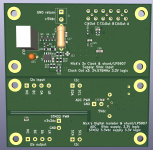
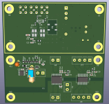
I've essentially finished the design - I need to double check the pins against the data sheets for the ICs etc. These can be populated by either a PL5907 with two caps or the shunt. There's also edges free of mask to make box. I've included a multi-turn borns pot for initial testing that way if the initial 10K resistor isn't right it can be trimmed then replaced by a new value.


You should add series terminator resistors to isolator I2S output. IME isolators outputs can have huge overshoots. What isolators are you planning to use?
i2s : MAX14434. 200Mbits/sec 3.3-5.5V logic. 4 channel, all single direction.
i2c : ISO1640QDWRQ1 which is designed for for i2c.
I did notice the overshoots with the i2s on the protoboard, so that's a good shout.
i2c : ISO1640QDWRQ1 which is designed for for i2c.
I did notice the overshoots with the i2s on the protoboard, so that's a good shout.
I've put in source series resistors, I've also added optional spaces on the underside for parallel termination (caps or resistors) to ground. The traces are matched from the IC pads to the resistor pad and then matched from the resistor pad to the connector pad.
I've not tried the i2c yet, however that would require bidirectional additions so I'll add the same for that.
I need to do some additions & modifications - the i2c needs pull-up resistors in place on both sides, and the demonstrator board for the MAX14434 has both R and C surface mounts to ground on both sides - I can adjust mine to get rid of the via (less inductance).
The i2c needs some careful calculation to ensure the draw is <3.5mA according to the datasheet: https://www.ti.com/lit/an/slva689/slva689.pdf so a 1K resistor seems to be right for the 400kHz with minimal load as a starting point.
The i2c needs some careful calculation to ensure the draw is <3.5mA according to the datasheet: https://www.ti.com/lit/an/slva689/slva689.pdf so a 1K resistor seems to be right for the 400kHz with minimal load as a starting point.
Last edited:
Boards have arrived. Plan is to test some of the impedances and reflections using a signal generator and scope. I calculated some resistors but before i order them I’ll cross check with some measurements.
Attachments
So I wanted to test the clock buffer - I have the basics for the RF filters installed, the SDG is pumping in a 2V 24.576MHz signal onto the pad of the CCHD (not currently installed - I'm not risking it until I know all is well with 3.3V). The SMPS bench supply is providing 3.3Vdc straight in. I'm more concerned - does it work! There's also very little noise coming back to the power supply which is nice.
The blue trace is the output form the buffer on a 50R termination (that's the larger signal) although it's through a 75R BNC. I'm interested in the shape and that looks rather good. I've plugged in some components that I had (the right value and sizes) for the filter components etc. I just need to now sort out the termination to accept 3.3V and not get reflections and 3.3V output.

Not bad for my first ever PCB design and a 4 layer at that. Note the cables aren't entirely the same length etc to the scope. Also the incoming was with a probe and the output via direct SMB->BNC 75R-> 50R termination hence the 1x.
So I think I can now calculate the values of the resistors needed to give me 50R. However that's for another day.
The blue trace is the output form the buffer on a 50R termination (that's the larger signal) although it's through a 75R BNC. I'm interested in the shape and that looks rather good. I've plugged in some components that I had (the right value and sizes) for the filter components etc. I just need to now sort out the termination to accept 3.3V and not get reflections and 3.3V output.
Not bad for my first ever PCB design and a 4 layer at that. Note the cables aren't entirely the same length etc to the scope. Also the incoming was with a probe and the output via direct SMB->BNC 75R-> 50R termination hence the 1x.
So I think I can now calculate the values of the resistors needed to give me 50R. However that's for another day.
Looks good. Did you "hack" your scope? Its pretty simple. I did mine (same model). The performance is excellent within its bandwidth. However to see the reflections inside a 75 Ohm BNC needs much faster hardware. At 1nS/foot the total time the wave is inside the connector is maybe 100 pS. With a 200 MHz scope you will see some resituals but not the inner details. However none of the parts you are using would see those either.
There are specific techniques for adjusting trace lengths. The wiggles you used will add inductance which could be an issue on at 10 Gbps HDMI signal. Probably irrelevent for digital audio.
There are specific techniques for adjusting trace lengths. The wiggles you used will add inductance which could be an issue on at 10 Gbps HDMI signal. Probably irrelevent for digital audio.
Yep it’s hacked to 200Mhz and the internets (eevblog etc) seems to think the scope’s frontend is about 250-280Mhz max. I wanted to explore some ideas with 25-50MHz so 5x means it’s going to give me a starting point. I don’t think the wife would approve a new scope!
The 75ohm BNC is is just the cable I bought by accident, it’a not 75ohm but as you know it has characteristics to match - I should get myself a 50ohm BNC cable.
The 75ohm BNC is is just the cable I bought by accident, it’a not 75ohm but as you know it has characteristics to match - I should get myself a 50ohm BNC cable.
To get meaningful data you need a TDR with sub 100 pS risetime. And a bunch of other odd stuff, or a network analyzer. And unless you are moving data at really high rates it doesn't matter much. To beter investmnets would be a Nanovna https://www.amazon.com/s?k=nanovna&crid=Q2N17TWQ95F6&sprefix=nanovna,aps,144&ref=nb_sb_noss_1 and a TinySA https://www.amazon.com/Portable-Tin...9Y2xpY2tSZWRpcmVjdCZkb05vdExvZ0NsaWNrPXRydWU=
You can see more useful stuff with these. The TinySA + some antenna can help find all the radiated junk that has a more deleterious effect on audio than bad jitter and the VNA will show the discontinuites in the connections.
You can see more useful stuff with these. The TinySA + some antenna can help find all the radiated junk that has a more deleterious effect on audio than bad jitter and the VNA will show the discontinuites in the connections.
Me too. My old HP54645D is only 2CH, sometimes I need more.Looks good. Did you "hack" your scope? Its pretty simple. I did mine (same model).
SDS1104 is good, but for analog signals is too noisy. Sometimes this is important.
So this is without the 15mF caps on the SMPS power supply - but this is running on my clock and isolator (the wiring needs cleaning up too and a few other things as the 3.3V is using the SMPS too at this stage). That's cleaner than the original SDG without the caps etc.
I need to verify that the clocking is equal too but it looked good from the scope.
So I'm not running the 15mF caps on this first run but it's the first run of my clock PCB and isolator PCB hooked up to the 3.3V on the SMPS supply instead of the 3080 with a second dropping that from 5.0 to 3.3V. Not bad for its first run with a patchwork of wires, sat next to the mains cables (literally next to the plug blocks). It seems less noise peaks are present looking between the two images.

That LF slope and the spikes should be resolved with the 15mF caps and using the 5.0-3.3V supplies.
Starting look clean (and about maxing out my ability to get it cleaner).
I need to verify that the clocking is equal too but it looked good from the scope.
Hehe putting the 15mF caps across the input for the regulators (between the SMPS and the regulator) has resulted in this lovely display:
View attachment 1151457
That's a considerable reduction in LF noise which is good.
So I'm not running the 15mF caps on this first run but it's the first run of my clock PCB and isolator PCB hooked up to the 3.3V on the SMPS supply instead of the 3080 with a second dropping that from 5.0 to 3.3V. Not bad for its first run with a patchwork of wires, sat next to the mains cables (literally next to the plug blocks). It seems less noise peaks are present looking between the two images.
That LF slope and the spikes should be resolved with the 15mF caps and using the 5.0-3.3V supplies.
Starting look clean (and about maxing out my ability to get it cleaner).
With just the added 15mF caps in (still have the 3.3V on SMPS direct without PSRR... and left to stabilise/warm up - this is a nice image 😀
One last one for a while I promise 🙂

I also tried a single ended SDG generated 1KHz signal and compared to a previous test (where the previous had the SDG also generating the master clock) - left is new with the new clock etc and right with the SDG master clock.
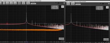
There is a subtle difference - it seems the noise is less allowing you to see more spaces (rendered) between the noise spikes and if you look at the 1KHz skirt there is a small narrowing if you follow the line. This is more noticeable further up the spectrum but a 1KHz signal phase noise distribution doesn't really make too much difference. It does show there's some reduction of noise based on the rough general upgrade.
I'd say the biggest drop of noise was from the isolator (27dB), then the 15mF and regulators on the power supplies (lowing LF noise), the clock is more polishing and the noise reduction. This goes well with what your point about - you will gain more in reducing power supply noise than simply reducing phase noise further. In the end the ADC/DAC then limits by it's internal noise.
The next steps for me are to add the bits and bobs I need to finish off the power supply, neaten and mount the internal boards etc in more secure way and then finally it can be a standalone unit. After that it's adding the i2c configuration and reset into the STM code and that's it basically done.
I also tried a single ended SDG generated 1KHz signal and compared to a previous test (where the previous had the SDG also generating the master clock) - left is new with the new clock etc and right with the SDG master clock.

There is a subtle difference - it seems the noise is less allowing you to see more spaces (rendered) between the noise spikes and if you look at the 1KHz skirt there is a small narrowing if you follow the line. This is more noticeable further up the spectrum but a 1KHz signal phase noise distribution doesn't really make too much difference. It does show there's some reduction of noise based on the rough general upgrade.
I'd say the biggest drop of noise was from the isolator (27dB), then the 15mF and regulators on the power supplies (lowing LF noise), the clock is more polishing and the noise reduction. This goes well with what your point about - you will gain more in reducing power supply noise than simply reducing phase noise further. In the end the ADC/DAC then limits by it's internal noise.
The next steps for me are to add the bits and bobs I need to finish off the power supply, neaten and mount the internal boards etc in more secure way and then finally it can be a standalone unit. After that it's adding the i2c configuration and reset into the STM code and that's it basically done.
Last edited:
I had a bit of time last night, and a couple of things/improvements (note I still need to order the additional bits but I figured I'd use components I had already):
1. Fitting the isolator decoupling caps - the iso chips didn't have any decoupling which would make them very noisy. (see image circle below)
2. Fitted the clock face down in its final position.
3. Wired up the i2s ribbon ground lanes and rerouted the it.
4. I'm also thinking about changing the larger 25MHz common mode chokes to the 600R 25Mhz inductors to reduce noise - I specifically left the vias uncovered so they can act as solder pads should I want/need them. In this case I can add caps in red to the make a RCLCLCLCLCLC chain rather than the current two inductors - see the image below. The caps will simply bridge to the nearest ground via. (the original filter was RLCLCLC only).
5. I noted that the inductor after R25 (the main power feed) didn't have a cap so this needs adding:

The improvement, just with the positioning and additional decoupling caps, seems to reduce the peak noise substantially after warming up - the space between the peak and the 16x average values has reduced which is is a good indication of overall noise reduction:
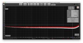
I think adding some small caps to decouple the ADC and the clock further (ie small electrolytics and ceramics) will help reduce the inductance of the long test leads further. However I think the next step is making some shielding around the ADC board.
1. Fitting the isolator decoupling caps - the iso chips didn't have any decoupling which would make them very noisy. (see image circle below)
2. Fitted the clock face down in its final position.
3. Wired up the i2s ribbon ground lanes and rerouted the it.
4. I'm also thinking about changing the larger 25MHz common mode chokes to the 600R 25Mhz inductors to reduce noise - I specifically left the vias uncovered so they can act as solder pads should I want/need them. In this case I can add caps in red to the make a RCLCLCLCLCLC chain rather than the current two inductors - see the image below. The caps will simply bridge to the nearest ground via. (the original filter was RLCLCLC only).
5. I noted that the inductor after R25 (the main power feed) didn't have a cap so this needs adding:
The improvement, just with the positioning and additional decoupling caps, seems to reduce the peak noise substantially after warming up - the space between the peak and the 16x average values has reduced which is is a good indication of overall noise reduction:

I think adding some small caps to decouple the ADC and the clock further (ie small electrolytics and ceramics) will help reduce the inductance of the long test leads further. However I think the next step is making some shielding around the ADC board.
- Home
- Design & Build
- Equipment & Tools
- Nick's audio test system (AK5572 ADC 129KHz 32bit stereo balanced input)

