@ MartinX
Your pcb accommodates your features in need IE specific capacitors and so on but has many audiophile or audiofool if you like mistakes ...there is a bunch of things to be done in a better way while some of them are very critical .
@cucicu
---I have never listened or tested original PCB next to mine ....since 2006 that i deal with P3A i have tested numerous versions of boards with some exactly like yours as a starting point .On e thing i can verify like all amplifiers and for CFP a bit more PCB structure and arrangement can and will play significant role when you look at the numbers in detail .
---Hum issue has to do with wiring and ground arrangement find the source and kill it there ! A double winding /rectifier is a very nice thing to do but the P3A is dead quiet even without it ...check how you ground things in the case ..
---Many times in the past i was asked to give away PCB and /or publish my designs It is a thing that i will not do ( pictures may be ) since where i stand from i will do nothing to harm Rod's pcb business or promote them in some other way .
Pictures ? yes ... tell me which version you like to see i got about 30 ..i will post a picture of the one that measured and played the best though the board is an integrated amplifier with preamp and source selector and features a few more goodies that are not included in the original schematic .
Attachments

Last edited:
I think you will not harm Mr.Elliot and his work publishing your layout...it is yours!
Indeed Rod's layout is visible on his site, looking with attention it is possible to reproduce it. Clearly visible in his site.
But I will not do that...
Indeed Rod's layout is visible on his site, looking with attention it is possible to reproduce it. Clearly visible in his site.
But I will not do that...
I am running out of time
What i would truly like to do is to make a P3A ala alchemist forseti meaning 4 output transistors including with each one a dedicated driver...
In simulation circuit is working but in real life it will have complications still i would like to try ..
Kindest regards
Sakis
What i would truly like to do is to make a P3A ala alchemist forseti meaning 4 output transistors including with each one a dedicated driver...
In simulation circuit is working but in real life it will have complications still i would like to try ..
Kindest regards
Sakis
The same old awful song!
Why don't you try to change the arguments? Instead of quarreling, how about doing real DIY? Let Rod Elliott be happy with his job, and us with our fanatism for DIY audio!
Why don't you try to change the arguments? Instead of quarreling, how about doing real DIY? Let Rod Elliott be happy with his job, and us with our fanatism for DIY audio!
@ MartinX
Your pcb accommodates your features in need IE specific capacitors and so on but has many audiophile or audiofool if you like mistakes ...there is a bunch of things to be done in a better way while some of them are very critical .
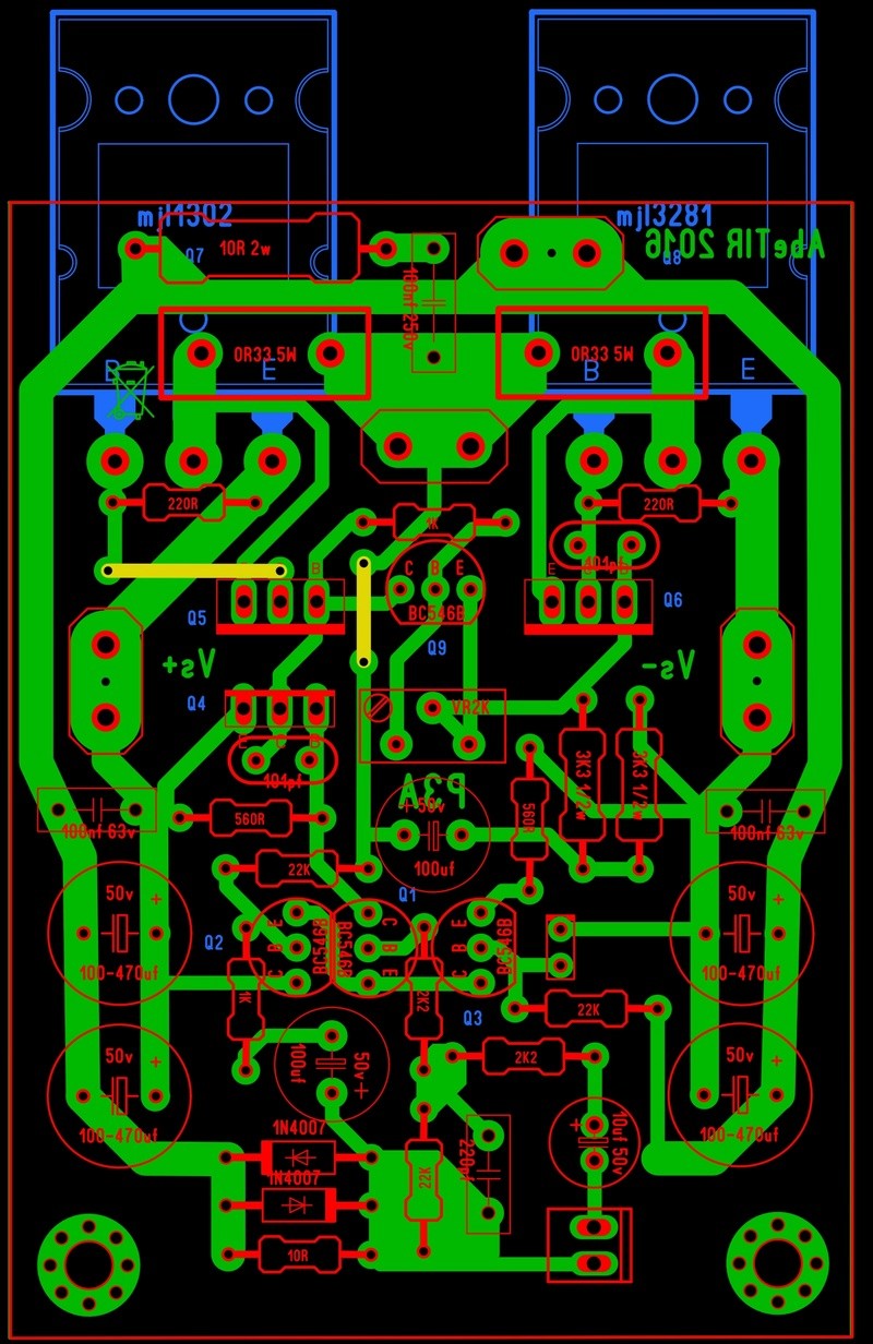
Would you care to mention some of the mistakes? I already know Q9 should be closer to one of the driver transistors for thermal stability, I discovered this when I already etched the board but I used it anyway thinking that it might be fixed with a somewhat elaborate piece of heat sink between the transistors, I never got around to do it and I have monitored the quiescent current and it is remarkably stable as it is.
I also use an output fuse, the feedback is taken off after the fuse so its sonic impact should be small, looking through fuse data sheet makes it clear all fuses are not created equal, the worst ones having significantly higher resistance for a given current rating.
Yes why not ...
But please make it bigger doesn't specially have to be that small ,then you will find place to locate 100nf/100R elsewhere ....you may as well skip it totally and relocate it in the binding post ...
Let me share some pcb experience
As long as you go for separate pcb for the power supply and you hardwire from here to there more or less most of the pcb presented previously in the forum will do .
There is going to be difference between them in the area of LTP , current source and ground distribution , location of miller caps and finally the way you choose to operate your Vbe and drivers ....
This can and will produce audible difference and measurable difference ....
\
Obviously this apply together with the rest of small details like matching choice of parts and so on ....
Now if you really choose to go with capacitors next to transistor there impact is 10 times more and difference is far more audible and measurable ...Difference is measurable and audible even if emitters are fed with a single line or fed with a triangle style line with the top of the triangle on the emitter and the base on supply capacitor .
Now please notice that here we talk about details ... from one detail you gain 2% from one other 4 and so on and on.
Point is that details of that style in the end are added and you come with a difference of 20% which is a very nice target to achieve.I expect all other PCB to play also very nice But if you look in depth you will actually see that this issue is far more critical than most people think .
Kindest regards
Sakis
@Smartix 21
I will not even bother to comment on your post ...I will only point that in the diy community world wide to my opinion nobody bothered to take the time to write down in so many details about so many circuits . Rod is not my personal friend or anything like that ...So actually i don't care much ...Inside my brain though i think that every diyer in electronics ( not only audio ) should donate to his site 1usd that will be enough
My opinion about this issue .
Last edited:
Mamy thanks for your answer..so do you think is a good idea to make a single pcb with amp,ps and dc prot all in one?
This is my opinion yes
DC protection may kept away ...dont like relays in my output anyway ...
OK...
if I post my all-in-one layout, would you gimme your opinion anyway?
regards
Member
Joined 2009
Paid Member
If you do use a relay you should also look to Rod Elliot's implementation where the relay switches the speaker load to ground and there are a diode + zener across the coil to speed up the turn-off.
If you do use a relay you should also look to Rod Elliot's implementation where the relay switches the speaker load to ground and there are a diode + zener across the coil to speed up the turn-off.
thanks
have you a schematic?
I put my P3A on the scope recently and noticed that negative side of sine wave has parasitic oscillation on both channels. I was curious about that and main suspects was combination of the semis I used Unisonic (2SD669a, 2SB649a) and Toshiba (2SC5200, 2SA1943). I decided to add another 100pF to C6 from the print side of the board. This measure solved the problem of parasitic oscillation on the negative side of sine wave. The conclusion is that with some combination of semis builder will need 200pF for C6 (not 100pF as on the original schematic).
Ian Finch was absolutely right that this topology is very tricky as far as the compensation is concerned. Unless builder has scope this parasitic oscillation would pass unnoticed because there is no way that during low level home listening user would hear it.
This quote is from Rod Elliott's article about "Compound Pair vs. Darlington Pair":
For reasons that I have always found obscure and somewhat mysterious, I've found that every amp I've designed using this configuration has parasitic oscillations on the negative half, and the addition of a small capacitor has been necessary every time. Strangely, I've never had an issue with parasitic oscillation with quasi-complementary amps, even though the negative side uses an identical compound pair. It makes no difference which side is driven (NPN or PNP voltage amplifier transistor) and which has the current source, and nor does it matter if the current source is active or bootstrapped. Only the negative side ever shows any sign of parasitic instability, and a small cap (typically 220pF) installed as shown stops it completely.
I put my P3A on the scope recently and noticed that negative side of sine wave has parasitic oscillation on both channels. I was curious about that and main suspects was combination of the semis I used Unisonic (2SD669a, 2SB649a) and Toshiba (2SC5200, 2SA1943). I decided to add another 100pF to C6 from the print side of the board. This measure solved the problem of parasitic oscillation on the negative side of sine wave. The conclusion is that with some combination of semis builder will need 200pF for C6 (not 100pF as on the original schematic).
Ian Finch was absolutely right that this topology is very tricky as far as the compensation is concerned. Unless builder has scope this parasitic oscillation would pass unnoticed because there is no way that during low level home listening user would hear it.
This quote is from Rod Elliott's article about "Compound Pair vs. Darlington Pair":
For reasons that I have always found obscure and somewhat mysterious, I've found that every amp I've designed using this configuration has parasitic oscillations on the negative half, and the addition of a small capacitor has been necessary every time. Strangely, I've never had an issue with parasitic oscillation with quasi-complementary amps, even though the negative side uses an identical compound pair. It makes no difference which side is driven (NPN or PNP voltage amplifier transistor) and which has the current source, and nor does it matter if the current source is active or bootstrapped. Only the negative side ever shows any sign of parasitic instability, and a small cap (typically 220pF) installed as shown stops it completely.
Hello , do you have tips how to detect this oscillation ? I have two p3a and I have access to
an oscilloscope.
Thanks
Unfortunately I did not take a photo of sine wave on the scope before I solved the problem. But it is not difficult to see it. On the lower (negative) peak of the sine wave form, the peak will look thicker in the up and down direction. You need to have a output sine signal of several volts p/p to see it clearly.
I would be very interested to know what type of capacitor you used ?
Kind regards
Sakis
I used NP0 multilayer ceramic 100pF/100V originally. That's what the cap was declared when I bought it. I measured it so I know that it had the right value, but I can not be sure if it is NP0 class. Additional cap I soldered on the print side of the board is the same cap, also measured.
Oscillation can be seen on the signal peaks of sinewaves and various effects as spikes and ripple on squarewaves. Here, the signal fundamental frequency is about 130Hz and the oscillation is significant so it's possible the effect of this supersonic oscillation could be audible.Hello , do you have tips how to detect this oscillation ?....
An externally hosted image should be here but it was not working when we last tested it.
I think many DIYs have stability problems because we have general difficulties understanding how linear amplifiers work. Sure, it's easy to follow a few simple expert guidelines or follow the audiophile parts mantras parroted on the web and still successfully build lots of gear. If we want reliable and stable performance when we don't have instruments to test properly though, it does mean we're stuck with following proven designs and parts specifications quite closely.
It is a big mistake to assume that we can just keep increasing HF gain by cranking up the Ft of semis without some penalty. It seems the P3a is OK with 30 MHz output transistors but combined with other increases to drivers and VAS, the stability turns ugly. Lets not ignore the effect of the VAS transistor's Cob on the Miller compensation capacitance. Checking that is a common omission.
On compensation caps - NPO thru-hole ceramic caps are now less common, with fewer and often unknown origins. Some are also doubtful quality in sizes over 50 pF (if even available). I think multilayer ceramics (COG type) are a more more reliable choice - Vishay for example, have a suitable range and that's what I now use.
Oscillation can be seen on the signal peaks of sinewaves and various effects as spikes and ripple on squarewaves. Here, the signal fundamental frequency is about 130Hz and the oscillation is significant so it's possible the effect of this supersonic oscillation could be audible.
An externally hosted image should be here but it was not working when we last tested it.
I think many DIYs have stability problems because we have general difficulties understanding how linear amplifiers work. Sure, it's easy to follow a few simple expert guidelines or follow the audiophile parts mantras parroted on the web and still successfully build lots of gear. If we want reliable and stable performance when we don't have instruments to test properly though, it does mean we're stuck with following proven designs and parts specifications quite closely.
It is a big mistake to assume that we can just keep increasing HF gain by cranking up the Ft of semis without some penalty. It seems the P3a is OK with 30 MHz output transistors but combined with other increases to drivers and VAS, the stability turns ugly. Lets not ignore the effect of the VAS transistor's Cob on the Miller compensation capacitance. Checking that is a common omission.
On compensation caps - NPO thru-hole ceramic caps are now less common, with fewer and often unknown origins. Some are also doubtful quality in sizes over 50 pF (if even available). I think multilayer ceramics (COG type) are a more more reliable choice - Vishay for example, have a suitable range and that's what I now use.
Thanks
I want to report improvement in sound quality after the negative side parasitic oscillation was fixed. Although ultrasonic oscillation was not audible per se, the amp now has superb clarity and sound staging. In fact, I am surprised how good this simple circuit sounds. I am convinced that even A class amp would not sound much better, and I am using only 10mV across both emiter resistors (15mA) bias.
I recommend caution and scope inspection if fast VAS, driver and output transistors are used.
I recommend caution and scope inspection if fast VAS, driver and output transistors are used.
- Home
- Amplifiers
- Solid State
- P3A Comparison table ( long .... )