I never noted a problem with temperature in my working Pearl 2, nor in the Minnie-Pearl. I have seen issues using JFET's in ULN amplifiers with 8 paralleled BF862's.
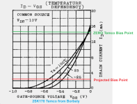
Erno Borbely had a chart from the 2sk170 datasheet which illustrated the optimal current for thermal stability -- that must have been a generation ago. (Borbely, JFETs the New Frontier Part 1). Not going to help us here.
You could use 3M copper tape to bind the 4 JFETs, attach to a small mass which will lend some hysteresis to the change in temperature.
(If you have ever made a DIY logarithmic amplifier, you probably used an NTC resistor to compensate for temperature changes)
Attachments
Hello All,
Sure the JFET's are temp sensitive, perhaps even the cascode transistors as well.
Building and measuring are all part of the learning and fun.
A while back I was testing JFET's with a Keysight B2912A SMU (a power supply that also measures Amps down to multiple digits) I learned that IDSS would settle over several 10's of seconds, as in having a warm up interval. Some JFET's would settle higher over time and some the current would drift lower. If I remember correctly the J74 and K170 were examples. The data is on the other computer.
Even a breath of air would effect the measured current. I ended up putting the Test Jig inside a steel project box on the carpeted floor.
I noticed in the photo of the Pearl 3 that the JFET's were not surface mount but TO92's.
Thanks DT
Can the Pearl 3 SE and balanced outputs be driven concurrently?
Can they be plugged in but the line stages off?
This is my use case:
One single super duper turntable driving a single Pearl 3.
Pearl 3 SE output to an SE line stage, SE amp and speakers.
Pearl 3 Bal output to a Bal line stage, Bal amp and speakers.
I'd rather leave the Pearl outputs plugged in, not having to reach over when I want to switch system configuration.
@wayne
Hmmm... I've been trying to figure an elegant way to switch between single-ended and balanced inputs on a BA2018 preamp because I eventually hope to run a balanced-output DAC and a Pearl (original) phono stage into it.
Maybe I should just try the Pearl 3 and simplify the preamp build... [sigh]
Hmmm... I've been trying to figure an elegant way to switch between single-ended and balanced inputs on a BA2018 preamp because I eventually hope to run a balanced-output DAC and a Pearl (original) phono stage into it.
Maybe I should just try the Pearl 3 and simplify the preamp build... [sigh]
A few photos for fun

PCB overview. C16 (center low) is normally not stuffed, and C2 (lower left) I don't have any on hand so it’s in the order queue.
I think the best part of this design is it does not take any strange, hard-to-find capacitors in the RIAA. They are all 0.1uF, with 1.0uF as interstage capaictors, and a couple of pF caps to round out the mix. You want to use fancy caps? Go ahead, they might be a bit funky to mount, but what the heck… it’s DIY! Want an (IMO) better idea than blindly throwing money at boutique parts? Buy a Meag328 component tester and a bag full of the 0.1uF caps, and measure & match them channel to channel, and on exact value. Get your RIAA perfect.
😎

Toshiba 2SK209GR input Jfets. Yep, they are small. They are also in-production new Toshiba, quiet, perfect for the circuit and about $0.25/ea, not approximately $8.00-10.00/ea…
Yes, this would be a perfect application to use Toshiba 2SK170, if you have them. If not, don’t worry about it.")
(If you're still terrified about soldering surface mount, these are genuine - https://www.ebay.com/itm/2533809687...uid=3BXt12BJT3G&widget_ver=artemis&media=COPY

This is OPA1656. You can use a DIP-8 dual opamp instead of the SMD in this position. The decoupling SMD capacitors are ceramic 1uF in 0805 size. I’m using film 0.47uF in the C21, C22 positions because I had them on hand. The silk is marked for electrolytic 220uF/25V, But this is an extremely non-critical value.

This is the DRV135 balanced line driver IC. They are SMD only. Capacitors are the same 0805 1uF ceramic as in the other opamp position.
If you don’t need/want XLR output you may leave this empty.
PCB overview. C16 (center low) is normally not stuffed, and C2 (lower left) I don't have any on hand so it’s in the order queue.
I think the best part of this design is it does not take any strange, hard-to-find capacitors in the RIAA. They are all 0.1uF, with 1.0uF as interstage capaictors, and a couple of pF caps to round out the mix. You want to use fancy caps? Go ahead, they might be a bit funky to mount, but what the heck… it’s DIY! Want an (IMO) better idea than blindly throwing money at boutique parts? Buy a Meag328 component tester and a bag full of the 0.1uF caps, and measure & match them channel to channel, and on exact value. Get your RIAA perfect.
😎
Toshiba 2SK209GR input Jfets. Yep, they are small. They are also in-production new Toshiba, quiet, perfect for the circuit and about $0.25/ea, not approximately $8.00-10.00/ea…
Yes, this would be a perfect application to use Toshiba 2SK170, if you have them. If not, don’t worry about it.
(If you're still terrified about soldering surface mount, these are genuine - https://www.ebay.com/itm/2533809687...uid=3BXt12BJT3G&widget_ver=artemis&media=COPY
This is OPA1656. You can use a DIP-8 dual opamp instead of the SMD in this position. The decoupling SMD capacitors are ceramic 1uF in 0805 size. I’m using film 0.47uF in the C21, C22 positions because I had them on hand. The silk is marked for electrolytic 220uF/25V, But this is an extremely non-critical value.
This is the DRV135 balanced line driver IC. They are SMD only. Capacitors are the same 0805 1uF ceramic as in the other opamp position.
If you don’t need/want XLR output you may leave this empty.
Last edited:
But when you parallel JFETs you want then closely matched?
Then you need a batch of 2SK209GR to select from?
I can see that RS has a good price on 3000 pcs......but that sums up.....even that they are cheap.....
Could be fun to build even that I don't have a turntable......
Then you need a batch of 2SK209GR to select from?
I can see that RS has a good price on 3000 pcs......but that sums up.....even that they are cheap.....
Could be fun to build even that I don't have a turntable......
A few more photos to help the early builders -

The TTA004 and TTC004 face their names on the silkscreen. Pinout is marked as well.

The jumper is installed here. Open for high gain (MC) closed for low gain (MM).

The unmarked hole in the center of the PCB is the main signal ground, attach to the turntable ground post on the chassis.
The TTA004 and TTC004 face their names on the silkscreen. Pinout is marked as well.
The jumper is installed here. Open for high gain (MC) closed for low gain (MM).
The unmarked hole in the center of the PCB is the main signal ground, attach to the turntable ground post on the chassis.
Last edited:
- Home
- Amplifiers
- Pass Labs
- Pearl 3 Burning Amp 2023