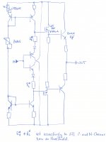
Well, they have more than that across them.
You're right, I just looked at the left of the schematic and missed the power supply connections on the right
 it's written "+31V".
> Another you would like would be the original Lightstar. The quiescent supply is 12.5 VDC approximately (bipolar) and it tracks the audio up to about 125 VDC bipolar. They use switching Mosfets at very high frequencies and call that a "down converter" using pulse width modulation.
Yeah I thought about using two cheap IRS2092 class D chips to make 2 tracking rails but honestly that's way over engineering and asking for trouble, because I don't need a high power amp. Also at lower Vce the collector capacitance of the devices increases, which means more switching noise would go through.
There was this idea Non-switching complimentary output stage
maybe you can get it working. Maybe two 9V batteries for the bootstrap supplies?
Thanks
will look into it.No. 153 at the bottom is a 1.2 V bias circuit with thermal stabilization.
OK, thermaltraks with no emitter resistors, but there is a 2200µF cap between the output transistor bases to allow the upside down diamond buffers to drive both output bases which is a nice idea... also the drivers are the same as the outputs, so their hFe mismatch should cancel at crossover, if hFe is well matched between devices. That's a cool idea.
I noticed that previously, with drivers and inductive resistors, there were two spikes per crossover. Now, without drivers and with non-inductive resistors, there is only one. So, I'm running a test with drivers and non-inductive resistors to see if that mess came from the inductance.
Last edited:
Hi peufeu,
You're actually going a long way into showing how these components interact. You're breaking new ground in public as I suspect many have done in private. I bet Nelson Pass has done this already too.
Using non-inductive emitter resistors at low value was one of my secret things to do. Mostly 0R22 and 0R1 values. Only really horrible amplifiers ran at 0R47 with the exception of Nelson's Stasis design. I wonder why the most common value was 0R33? My guess would be bias stability without too much work using smaller heat sinks than they should have.
Using non-inductive emitter resistors at low value was one of my secret things to do.
Extra line added in my amp upgrade list: Mills mra05 0r22: 30pcs @ €3,6/pc.
Thank you peufeu, very interesting.
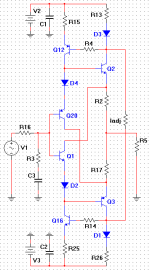
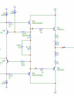
You may use a hybrid diamond buffer, with the drivers in between being Lateral Fet's. So you have a certain isolation between VAS and output, and the buffer could be driven from a single point without the need of a bias spreader.
The diodes for biasing could be the ThermalTrak diodes.
See the quickly drawn schematic.
To ensure sufficient voltage swing, the driver circuit could have higher rails than the output circuit.
Here some thoughts re "speed up" caps between driver emitters/sources
Might Diamonds
I add also a "distortion reducer circuit" I found somwhere (credits to unknown) for a diamond buffer.
Attachments
Hi peufeu,
You're actually going a long way into showing how these components interact. You're breaking new ground in public as I suspect many have done in private. I bet Nelson Pass has done this already too.
I suspect so lol. Well, I don't mind sharing the secret sauce.
Extra line added in my amp upgrade list: Mills mra05 0r22: 30pcs @ €3,6/pc.
I measured this one: 16nH, quite low. And I noticed it was not even the non-inductive model.
These are quite pricey though, 1W SMD ones are 9c each by 100 but they need a vertical mounted PCB for convection, otherwise they will just cook.
You may use a hybrid diamond buffer, with the drivers in between being Lateral Fet's. So you have a certain isolation between VAS and output, and the buffer could be driven from a single point without the need of a bias spreader.
The diodes for biasing could be the ThermalTrak diodes.
See the quickly drawn schematic.
To ensure sufficient voltage swing, the driver circuit could have higher rails than the output circuit.
Yeah, it gets complicated, and you need a substantial boosted supply because the lateral FETs suck at low Vgs,
Here some thoughts re "speed up" caps between driver emitters/sources Might Diamonds
I add also a "distortion reducer circuit" I found somwhere (credits to unknown) for a diamond buffer.
Unfortunately the big cap between the diamond emitters will discharge during a half period of low frequency if it has to give substantial base current to the power devices, but it can only recharge through the current sources, so it risks being underbiased for a while after that... and while voltage on the cap is lower than it should, one of the drivers will turn off completely (see my next post). So that requires a large driver bias current anyway, at which point, above 100mA, one pair of vertical FETs biased at the same current becomes interesting...
So. The drivers.
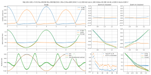
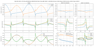
On all the following plots, the top row is labeled "Ie" but it is actually the base current of the power devices, because I moved the probes there. The second row is the base current of the drivers.
MJLs biased at 50mA, 0R15 emitter resistors. MJL15030/1 drivers.
This is with 150R resistor between driver emitters, so 8mA idle current.
The power devices make one base current spike at turn-off, but the drivers make two, one at turn-on, and one at turn-off. Both spikes are joined together, so they look like one big lumpy mess.
One pic has the 100nF cap between emitter bases, the other doesn't. It does lower the high harmonics a little bit, but the mess is still there.
Attachments
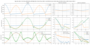
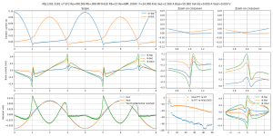
Increasing driver bias to 33mA reduces the size of the mess, but does not solve the problem.
The worst case seems to be when there is not enough driver bias, and when one transistor needs to turn off and needs charge pulled out of its base... but its driver can't pull current in that direction, so it turns off. So driver bias influences HF distortion.
The worst case seems to be when there is not enough driver bias, and when one transistor needs to turn off and needs charge pulled out of its base... but its driver can't pull current in that direction, so it turns off. So driver bias influences HF distortion.
Attachments
Last edited:
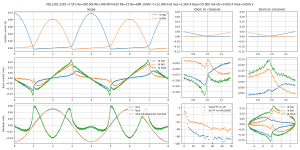
Faster drivers (C5706/A2039) really help. Also their hFe is well matched, which means the input current is much less distorted even outside of the crossover.
With these faster drivers the difference between PNP and NPN, which was previously small, now becomes obvious: the NPNs turn off cleanly while the PNPs make a mess. So that's one point for Circlophone.
With these faster drivers the difference between PNP and NPN, which was previously small, now becomes obvious: the NPNs turn off cleanly while the PNPs make a mess. So that's one point for Circlophone.
Attachments
But does it matter? I'm not sure.
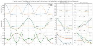
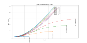
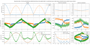
These are more realistic (for audio) currents and frequencies. Crossover turn-off spike distortion begins to manifest at 12kHz and 1.28A, it is not present at 8kHz.
So... while the non-switching topologies would probably look better at unrealistic high frequency/current, will they bring actual benefit?
Still, input current looks a lot better with the matched hfe drivers.
> (C5706/A2039)
For cascode use only, but there are other high fT transistors... and mosfets.
Attachments
I will try this biasing topology.
Unlike the usual Vbe multiplier, it ignores driver Vbe, so it should drift less. But it has another advantage: since it keeps the voltage between driver emitters constant, it allows putting a large capacitor there without causing problems like the standard topology does. This means the driver on the other side will be able to assist in turning off the power transistor.
It also has advantages for my setup: it should run at the same bias no matter what the driver type (bipolar or MOSFET), which is an advantage for testing, although the software already sets the bias. In this topology, bias is adjustable by sticking a pot between the bases of Q5 and Q6 (which also changes mV/°C), or with a current source which adds voltage on top of base resistor R16 (which does not change mV/°C).
Attachments
Last edited:
An externally hosted image should be here but it was not working when we last tested it.
Bias VT4 Ge (HF)\VT5
Last edited:
You mean low Vds right?Yeah, it gets complicated, and you need a substantial boosted supply because the lateral FETs suck at low Vgs[...]
I thought vertical FET's suck even more at low Vds....
Yes, Vds, sorry about that. At low Vds, capacitance of these ALF lateral FETs increases less than IRFP9/240 verticals at low Vds, but they lose more gm and they can't deliver high current. So both will waste the last volts, but for a different reason.
Attachments
I only tested up to 1 amp, it would be worse at higher currents. The N channel behaves quite the same. But what I don't like about these FETs is the sharp changes in gm during crossover, which create much more high order distortion than the vertical FETs.
I've uploaded all the results here:
https://www.diyaudio.com/forums/sol...ed-transistor-measurements-4.html#post6734939
Note some graphs only go to 5V Vce so if you don't see it losing gm, make sure you look at the Vce legend. FETs are labeled like BJTs, so it is not labeled Vds, but you get the idea.
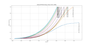
This is the MJLs being driven by IRF610/9610.
100nF cap between both sources, 130R gate resistors for the FETs.
I'm not convinced by the FET performance on these crossover spikes.
The FETs will need a bootstrapped power supply because their capacitance increases too much at low Vds. It would be a shame to use MJLs, which perform well at low Vce, and waste 10V headroom due to the FET drivers. But using a bootstrapped supply means it is possible to use the fast low-voltage A2039/C5706 instead, and they perform better as drivers than these FETs.
Of course at lower frequency/current where no crossover spikes occur, the much higher current gain of the FETs would still be an advantage, so it's all about tradeoffs.
Attachments
-
 scope-Bias=50.000 mA Iout=2.560 A F=48.000 kHz MJL1302-3281 v7 EF2 Re=0R15NI Rb=3R8 IRF9-610 Rb=.png277.2 KB · Views: 56
 -
 scope-Bias=50.000 mA Iout=2.560 A F=24.000 kHz MJL1302-3281 v7 EF2 Re=0R15NI Rb=3R8 IRF9-610 Rb=.png289.3 KB · Views: 54
 -
 scope-Bias=50.000 mA Iout=2.560 A F=12.000 kHz MJL1302-3281 v7 EF2 Re=0R15NI Rb=3R8 IRF9-610 Rb=.png317.9 KB · Views: 59
 -
 scope-Bias=50.000 mA Iout=2.560 A F=6.000 kHz MJL1302-3281 v7 EF2 Re=0R15NI Rb=3R8 IRF9-610 Rb=1.png348.4 KB · Views: 74
 -
 scope-Bias=50.000 mA Iout=1.280 A F=24.000 kHz MJL1302-3281 v7 EF2 Re=0R15NI Rb=3R8 IRF9-610 Rb=.png300.4 KB · Views: 99
I've seen enough crossover spikes for now. So it will either be several tiny C5200/A2907 in parallel with MOSFET cascode, or MOSFETs, or some non-switching business.
Ian mailed me Cordell's bias stability equation, which I already know about, but I had forgotten the part about the thermal impedance through the heatsink to the Vbe multiplier transistor... So that gave me an idea to remove this bit. Time to measure how it works.
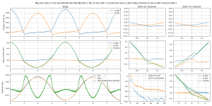
We have several bias sensors in competition.
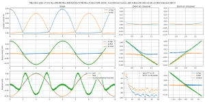
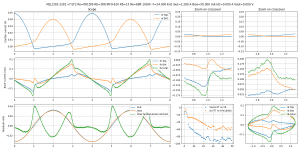
For this test, power supplies are 10V, and an auxiliary MOSFET switches a 7R5 resistor in the MJL3281 emitter, which causes a dissipation of 13W. The micro's ADC acquires Vbe of the power transistor for an instant measurement of temperature (blue trace), and it also acquires the candidate temperature sensors (orange trace). Do not look at the green curve for now.
BD139 on heatsink, as usual, 4cm away from the power device.

Vbe measurement gives a pretty damn good Thermal Resistance from Chip to Heat sink of about 0.5-0.6°C/W which is lower than datasheet. Either the gains are set wrong, or it's performing pretty well. Also Keratherm red really works.
The sensor transistor on the heatsink does not notice much.
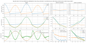
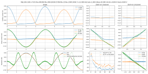
BD139 on heatsink, right next to the power device.

Now it reacts, but it takes a long time. Also its gain is low, it does not reach the same temperature as the MJL, so it will only correct about half the tempco of the power transistors. For a full correction, in this setup the temperature-dependent Vbe changes of the Vbe multiplier should have more gain that a Vbe multiplier allows when biasing BJTs. With MOSFETs though, there is enough gate voltage to set the Vbe multiplier to a high enough gain. Would it work?
The red curve is the result with gain applied. It shows that it hasn't settled yet after 82 seconds, so the algorithm that calculates the gain gets the wrong value. This is too slow.
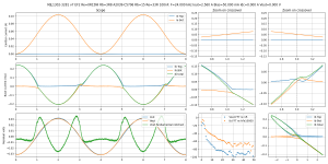
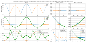
This time the MJL1302 is heating BD139 placed next to it on the heatsink. Still a solid mehhh.

The next sensors exploit the fact that the leadframe of the power transistor is connected to the center leg which is Collector. Therefore, heat from the silicon should go through that center leg as well as through the back, which means the collector leg should be a good place to sense junction temperature.
MMBT3904 soldered on collector lead of MJL3281 5mm away
It is soldered 5mm away from the MJL3281 package, where it would be if the power device was mounted on a PCB with short leads.
I wired it as a diode and I'm just measuring its Vbe. It is not part of the bias network. Being soldered on the collector of the power device, its own collector is at power supply voltage, which would require some level shifting to make it into a bias controller. Nothing too complicated though.

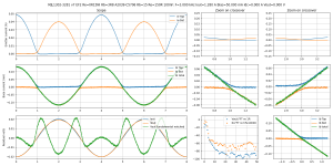
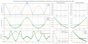
It works a lot better! It is much faster, requiring only a few seconds to react. It settles much quicker, which means the gain value in the plot would result in adequate and fast bias compensation.
I tried soldering it closer to the MJL3281 (it was previously 5mm away from the package). It is quite difficult even with the big soldering iron, because the pin soaks a lot of heat and the SOT23 does not cooperate:

It's even better.
SOT-89 PNP bipolar transistor directly soldered on collector lead of MJL1302
I thought, since the SOT89 has a thermal tab and the SOT23 does not, then it should work better.

It did not work better, most likely because I soldered it on a tiny PCB for convenience, so its thermal path to the power transistor was longer.
Ian mailed me Cordell's bias stability equation, which I already know about, but I had forgotten the part about the thermal impedance through the heatsink to the Vbe multiplier transistor... So that gave me an idea to remove this bit. Time to measure how it works.
We have several bias sensors in competition.
For this test, power supplies are 10V, and an auxiliary MOSFET switches a 7R5 resistor in the MJL3281 emitter, which causes a dissipation of 13W. The micro's ADC acquires Vbe of the power transistor for an instant measurement of temperature (blue trace), and it also acquires the candidate temperature sensors (orange trace). Do not look at the green curve for now.
BD139 on heatsink, as usual, 4cm away from the power device.
Vbe measurement gives a pretty damn good Thermal Resistance from Chip to Heat sink of about 0.5-0.6°C/W which is lower than datasheet. Either the gains are set wrong, or it's performing pretty well. Also Keratherm red really works.
The sensor transistor on the heatsink does not notice much.
BD139 on heatsink, right next to the power device.
Now it reacts, but it takes a long time. Also its gain is low, it does not reach the same temperature as the MJL, so it will only correct about half the tempco of the power transistors. For a full correction, in this setup the temperature-dependent Vbe changes of the Vbe multiplier should have more gain that a Vbe multiplier allows when biasing BJTs. With MOSFETs though, there is enough gate voltage to set the Vbe multiplier to a high enough gain. Would it work?
The red curve is the result with gain applied. It shows that it hasn't settled yet after 82 seconds, so the algorithm that calculates the gain gets the wrong value. This is too slow.
This time the MJL1302 is heating BD139 placed next to it on the heatsink. Still a solid mehhh.
The next sensors exploit the fact that the leadframe of the power transistor is connected to the center leg which is Collector. Therefore, heat from the silicon should go through that center leg as well as through the back, which means the collector leg should be a good place to sense junction temperature.
MMBT3904 soldered on collector lead of MJL3281 5mm away
It is soldered 5mm away from the MJL3281 package, where it would be if the power device was mounted on a PCB with short leads.
I wired it as a diode and I'm just measuring its Vbe. It is not part of the bias network. Being soldered on the collector of the power device, its own collector is at power supply voltage, which would require some level shifting to make it into a bias controller. Nothing too complicated though.
It works a lot better! It is much faster, requiring only a few seconds to react. It settles much quicker, which means the gain value in the plot would result in adequate and fast bias compensation.
I tried soldering it closer to the MJL3281 (it was previously 5mm away from the package). It is quite difficult even with the big soldering iron, because the pin soaks a lot of heat and the SOT23 does not cooperate:
It's even better.
SOT-89 PNP bipolar transistor directly soldered on collector lead of MJL1302
I thought, since the SOT89 has a thermal tab and the SOT23 does not, then it should work better.
It did not work better, most likely because I soldered it on a tiny PCB for convenience, so its thermal path to the power transistor was longer.
- Home
- Amplifiers
- Solid State
- Power amp OUTPUT STAGE measurements shootout