Hi. I volunteered to modify the crossover points of a crossover. Existing crossover points were 250Hz and 2500Hz.
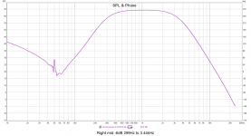
The 250Hz low pass sections look OK but in the mid-range and HF filters the response rises with decreasing frequency below about 60Hz. There would be significant drive at 20Hz and below to the MF drivers and tweeters.
Then I reverse-engineered the schematic shown below. It’s like nothing I’ve ever seen before.
You can see buffers and standard Sallen and Key 24dB Linkwitz-Riley 250Hz and 2500Hz low pass filters in there.
There are no standard Sallen and Key high-pass sections.
But what are IC2b, IC4a and IC6a and their associated resistors and capacitors? Simulating them in isolation shows they have a kind of peaked band-pass response.
IC4a doesn’t appear to be doing anything in that position and maybe should be in the high-pass section.
The output of some stages appears to be added/subtracted at various points.
The PCB is an old, custom single-sided affair with no resist or component markings. Maybe whoever layed it out made lots of mistakes.
Maybe I’ve made mistakes reverse-engineering the schematic but I’ve checked it a number of times.
Can anyone tell me what the designer might have been trying to achieve and what might be the advantage over a standard Sallen and Key topology?
Ultimately, I need to be able to change component values which is easy for the 2 low pass sections but not easy for the high pass sections.
Attachments


You sure there's not a cap in between the two 10k series feedback resistors to ground (in each of those red-circled sections)? Looks like it wants to be a bandpass filter with those strange two feedback resistors in series.
Last edited:
Looks to me they just wanted to simplify the BOM by doing almost everything with 10ks. Except the 47k input resistor. Build-out resistors would be mandatory for opamp stability into cables but 10k won't work well for that.
Thanks for the responses. I haven't got the 250Hz low pass and 2.5kHz low pass simulations to match what I'm measuring yet so I may some errors in the schematic.
I gave the schematic a good look-over. Didn't notice any schematic typos, so to speak. It looks like the high pass function is created by subtraction of an all-pass (not sure on this) from the low pass via R27. The trouble with subtraction is to get good stop-band rejection the gains of the two paths need to be well matched - chances are the re-emergence in the bass is due to insufficiently close tolerance resistors? This is just a guess as I've not simulated it, too lazy to type it all in 🙂
This is just a guess as I've not simulated it, too lazy to type it all in 🙂
Here's the LTSpice file.
Attachments
Thanks - looks like my hunch might have been correct - the high pass stop-band rejection degrades considerably when R27 is changed to 9k9. So resistor tolerance is critical.
Even with 10k the simulated HF response doesn't look great.Thanks - looks like my hunch might have been correct - the high pass stop-band rejection degrades considerably when R27 is changed to 9k9. So resistor tolerance is critical.
Attachments

The notch filter must be in there for a reason - that's implemented in the HP section by the (lowest) red circled opamp with the 3n3s. Again that's made by subtraction so will be tolerance sensitive to both Rs and Cs. You only have 8 points per octave set, you can try changing to 80 to see more detail.
- Home
- Source & Line
- Analog Line Level
- Reverse-engineered op amp crossover questions