hello,
I don't know how long was the commercial life of the Sansui Diamond-Differential system.
Some may love it, some may hate it. Because it adds a voltage amplifier stage at the input, which may cause stability issues.
To my suprise, I discovered that the Sansui Diamond-Differential regularly comes as a winner, when doing Spice simulations.
1.
It enables a straightforward JFET input stage powered by - and +12V rails at the input. The drains of the JFET input stage are loaded by relatively low resistances, making the gain moderate, making the frequency bandwith large. A voltage gain in the order of x5 ... x8 with drain resistances of 180 ohm defines a bandwith extending well beyond 10 MHz. So, effectively, this stage is not going to pervert stability.
2.
The Diamond-Differential takes the low impedance (high bandwidth) voltage swing coming from the collectors of the JFET input stage, and exploits it in such a manner that if there is a large voltage error, then the current that's conveyed to the VAS is an order of magnitude bigger than the Diamond-Differential quiescent current. This feature is unique. You can't get something like that using a dumb differential stage. Only the Diamond-Differential is capable of this. It means that the dV/dt is not anymore defined (limited) by the quiescient current of the intermediate stages. There may be a saturation occuring at the horizontal NPN-NPN level, as it it the rule with conventional differential stages. But here, the diagonal current that also flows from the NPN upper transistor to the PNP lower transistor, is not subjected to saturation. The diagonal channel is thus immune to satutation, and can dump tens of milliamps in the VAS base, in case of need.
3.
The VAS that has been used here is a self-biased cascode. The big advantage of the self-biased cascode, is that it enables you to freely define the VAS quiescent current. The VAS quiescent current in not anymore related to the VAS quiescent curent of the previous stage, and not anymore related to the way the previous stage got loaded.
It means that we can load the Diamond-Differential with current mirrors.
The voltage gain will thus be maximized.
Speed will be maximized, as now the VAS base can litteraly get short-circuited for fast turn-off.
The beauty of the self-biased cascode is that the cascode nearly comes from free, with a very simple arrangement. There are indeed 4 transistors instead of only 1 for a dumb VAS, but 3 of those transistors are inexpensive low voltage ones. The zener has been fitted for boosting the cascode voltage, in case one doesn't want to operate the whole stage at a nearly zero Vce voltage.
4.
The MOSFETs that have been used here are vertical ones, straight coming from Tina 7 Texas Instruments built-in database. I don't know how realistic their models are, for operating in the turn-on region (between 25mA and 100mA bias current in the MOSFETs).
5.
The MOSFET bais setting has been done using a complementary arrangement, to be thermally coupled to the MOSFETs, that may be expanded in the future for implementing a non-switching biasing scheme (aka Super-Linear in Hitachi folklore).
In this present implementation, there is a 100µF cap put in parallel with the bias voltage generator.
A future implementation, providing a non-switching biasing scheme, will modulate the bias voltage. Is this going to add distorsion ? Maybe the non-switching biasing scheme is a trap, bringing a lot of THD above 1 KHz. To be experimented on simulation.
Anyway, this structure provides a 130 dB open loop gain (200 Hz pole), and continues behaving like a perfect integrator well above 1 Mhz.
THD is 0,0021% on a 1 KHz sinus, with a voltage gain of x40.
Slew-rate looks more than adequate, with a voltage gain of x40.
There is absolutely no ringing on a 10 KHz square wave.
What makes me think that this arrangement is a healthy, quality one, is that one doesn't need to fiddle with compensation networks for getting Tina converging and for getting Tina drawing the transient response when feeding a 10 KHz square wave at the input.
However complicated it may look on paper, you will be surprised by the no-compromise approach this design allows. And you get a FET input stage, which is mandatory for an input capacitorless coupling.
One question : where can I buy a decent double N-FET, preferably low noise and low offset ? Where are they now ?
Feel free to play with the simulation file that is provided as attachement.
Any suggestion welcome.
Attachments

Last edited:
this comes from back in the days of the slew rate wars, right?
what was this one rated - a few hundred volts per microsecond?
some products during the slew rate wars had a reputation for bad clipping and recovery behaviors, like hard sticking to the power rails, often killing tweeters in the process. i don't recall if sansui products were in that group or not. maybe anatech could chime in about his experiences ...
i always wanted to get the service manual for the diamond differential power amp with mosfet outputs but sansui wouldn't sell it to me - something about the mosfets made them reluctant to release the service manual at the time.
by the way, have you use both tina and ltspice? if so, which do you like better?
thanks for sharing,
mlloyd1
I have used both Tina and LTspice. I prefear Tina because of the realtime features of Tina. One can measure a voltage with the oscilloscope and at the same time modify the value of a component. See attached .jpgBy the way, have you use both tina and ltspice? if so, which do you like better?
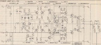
Also as attached .jpg, the schematic of the Sansui AU-D5, the Diamond-Differential amp.
Cheers,
Steph
Attachments

steph:
thanks for the comments.
here is a link to the patent for sansui's diamond differential in case you would like to read about it:
Patent US4229705
mlloyd1
thanks for the comments.
here is a link to the patent for sansui's diamond differential in case you would like to read about it:
Patent US4229705
mlloyd1
interesting patent. thanks!
link to currently available dual low noise n-channel jfets:
http://www.linearsystems.com/datasheets/LSK389.pdf
and
http://www.interfet.com/pdf/DS_IFN146.pdf
mlloyd1
link to currently available dual low noise n-channel jfets:
http://www.linearsystems.com/datasheets/LSK389.pdf
and
http://www.interfet.com/pdf/DS_IFN146.pdf
mlloyd1
If you like Tina 7 Texas Instruments, you may play with the non-switching evolution of the design. See attached .zip file.
The picture below shows the voltage on the 0,47 ohm source resistors. As you can see, both MOSFETs never go off. This non-switching arrangement samples the 0,47 ohm source resistor voltage drop of both MOSFETs, individually, and compares the voltage drop with a reference voltage. When the 0,47 ohm resistor voltage drop is less than the reference voltage, the non-switching arrangement sends a correction current into the base of the Vbe multiplier that's associated to the MOSFET.
This arrangement works on paper (on simulation).
The bias current is set by the voltage divisor connected on the reference voltage defined by the forward drop of a Schottky diode.
The loop gain of the correction can be adjusted by changing the values of the emitter resistors of the comparator.
The control loop is stable and doesn't require a compensation network for stability. The comparator and the control loop are so fast that the on/off comparator transitions are eaten by the input capacitance of the mosfet. The MOSFET source doesn't deliver any glitch associated to the on/off and off/on transistions of the comparator.
The more loop gain you put (emitter resistors equal to 100 ohm in the comparators), the more accurate the minimum bias current will be, in the MOSFET, independent of the instantaneous power that's delivered.
If you put less loop gain (emitter resistors equal to 330 ohm in the comparators), you allow the MOSFET to see a slight dynamic variation of the bias current, depending on the instantaneous output power. It sounds like a disadvantage, but if you look closely to the source current waveforms, you discover that a low loop gain enables the waveform to avoid a hard corner, when the changeover occurs. If you succeed in softening the changeover corner, then the copper tracks of your power stage will radiate less eletromagnetic waves, and it will induce less corruption in the high sensitivity stages like the differential input pair, the Diamond-Differential, and the VAS.
A Class-A amplifier never experiences changeover corners.
A Class-A amplifier doesn't need to generate and manage internal signals having a larger frequency bandwidth than the audio signal he is processing.
A Class-A amplifier copper track never radiates HF electromagnetic waves.
A Class-AB amplifier always experiences changeovers corners, when operated at a power greater than a few hundreds of milliwats (when the output current needs to be bigger than the output stage quiescent current).
A Class-AB amplifier absolutely needs to generate and manage internal signals having a larger frequency bandwidth than the audio signal he is processing.
Look again at the changeover corner of the source current. If you throw this wave into a spectrum analyzer, you will see that there is a considerable harmonic content (this is only half the audio wave), plus a massive energy content beyond the audio frequency band. And you absolutely need to convey this energy, low frequency plus high frequency, otherwise you will get crossover distortion.
But wait a minute, how can thus a Class-AB amplifier deliver a clean, low distorsion signal, with all those self-generated harmonics and out-of band signals ?
Answer : the additivity and the symmetry will save you. When you connect the NMOS source electrode on the PMOS source electrode, some magic occurs : the harmonics and the out-of-band phase energies do cancel. Both the NMOS and the PMOS had massive harmonics and HF content, but 180 degree phase shifted. If you connect them, adding the currents, you get a cancellation effect.
But remember : the cancellation effect only occurs at the point where the MOSFETs source electrodes do connect. Usually, this is where you connect the loudspeaker and the feedback network.
The MOSFETs gate copper tracks, the MOSFETs drain copper racks, the MOSFETs source copper tracks, and the power supplies copper tracks and wires still generate massive harmonics and HF elecromagnetic waves.
I'm producing all this litterature in order to avoid any misunderstandings about this proposed non-switching scheme.
Now everybody equipped with a brain will have understood that this non-switching scheme is not a Class-A emulation.
According to me, it only makes sense to tweak the proposed non-switching arrangement in one particular direction : softening the changeover corners. This idea is the most important idea for getting a Class-AB amplifier that sounds warm and precise.
See attached .zip file.
Any suggestion welcome for softening the changeover corners.
Attachments
-
Sansui Diamond-Differential with current mirror loads and self biased VAS cascodes and Non-Switc.zip109.5 KB · Views: 285
-
 Sansui Diamond-Differential with current mirror loads and self biased VAS cascodes and Non-Switc.jpg146.4 KB · Views: 1,828
 -
 Non-Switching bias for IRF vertical MOSFETs.jpg223 KB · Views: 1,690
Last edited:
Now this amp is getting the non-switching Class-AB softening add-on.
See attached Tina 7 Texas Instruments simulation file.
It is a development model (use of voltage sources and current sources). The bias control loop is now getting a variable loop gain. The loop gain is minimized when the instantaneous 0,47 ohm current is minimal. The trick is in the differential amplifier operating current. It is now variable so the dynamic Rbe varies accordingly (log relation), and come in series with the 180 ohm emitter resistors. The 180 ohm resistors define the maximal loop gain, when the dynamic Rbe become small in front of 180 ohm.
The waveforms look perfect with a 1KHz 500 mV signal at the input.
There are no hard corners nor inflexions anymore in the MOSFETs source currents.
All the edges are nicely softened.
When viewed from a certain distance, this may be confused with Class-A operation.
However, when one decreases the amplitude of the input signal, one can see that the overlap region of the MOSFETs source currents get somewhat dirty. Some edges are popping. I think this behaviour is caused by the log loop gain function. When the differential pair is operating at a very small current, like 50µA, the speed of the bias control loop degrades. And the precision of the current mirrors maybe degrades also. How to improve this ?
Do we need to significantly raise the nominal bias current (which was in the range of 50mA) ? Use 100 mA, 250 mA or 500mA ? That would be a shame, and would introduce a nasty idea that the amp is tuned for delivering clean audio above a certain listening level threshold. Need to avoid this !
Time to think about a long-term bias control, based on the audio signal that gets reproduced ? Seems like quick and lazy fix ... not improving the idea.
Any suggestion welcome.
Attachments

Last edited:
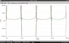
Looking closer at the (attached) 10 KHz waves, one can see the effect of the bias servo-loop experiencing a reduced speed around zero MOSFETs currents , especially in the leading edges.
Please note however how the trailing edges get nicely softened, not radiating high-frequency energy anymore.
It would be wonderful to get the leading edges the same quelity as the trailing edges.
How to tell the bias-servo loop "look out, there is a sharp edge coming, please prepare for action" ?
That's feedforward, actually.
A feedforward arrangement locally applied to both Bias servo-loops, independenty.
Sampling the MOSFET gate is a possible way. One can thus create an auxiliary signal path. We can differentiate the gate signal, and pulse a negative current into the bias-servo loop long tailed pair, for temporary increasing its voltage gain. This is how we may prepare it for action.
Problem is not to end-up with 10 Amp bias current when feeding the circuit with a 250 Khz square wave ... A low-pass filter at the amplifier input seems mandatory ... but is ineffective if 1st order and 50 KHz @ -3db ...
Anyway, the wole process is not linear anymore : conceptually, there is a kind of rectification needed, for not ruining the trailing edges. One must avoid temporary decreasing the the bias servo-loop long tailed pair on the trailing edges.
Any suggestion welcome.
Attachments
About the Class AB Soft Non-Switching,
http://www.diyaudio.com/forums/solid-state/163231-class-ab-soft-non-switching.html
http://www.diyaudio.com/forums/solid-state/163231-class-ab-soft-non-switching.html
Last edited by a moderator:
- Status
- Not open for further replies.
- Home
- Amplifiers
- Solid State
- Sansui Diamond-Differential with current mirror loads and self biased VAS cascodes