
With 330nF the +3dB point is ~200Hz.You want 400Hz, change the capacitor to 330/2 nF.Not quite sure how it works and what is the freq. response.
The higher the resistance the more temperature dependent it gets.But...
Can I rise the base resistor from 10k to 100k (and the 82k resistor I guess).
Try 47k.
Your schematic shows 3k3 😕There is a Jfet buffer just before the bass boost.
With a ..33k source resistor, for minimal consumption.
So, the output Z is low.
Be aware of two things.
Low output Z doesn't mean high drive capability, depends on the bias current.
The ouput level is max ~3Vpeak. With a bass boost of 10x the max input is 300mVpeak (200mVrms).And that 300mV goes for the other frequencies too.
Mona
Attachments

Seems the input impedance of Ketje's circuit is not a problem for the preceding buffer.
And it NAILS it on the simulation (with small values adjustment) !!!!
R20 - 50k is the volume pot, as it is connected now. 33k source resistor and 50k load.... It sounds ok as well.
Just wondering, it the consumption could be reduced.
The simulator shows 0.8-1mA.
The double jfet buffer consumes 0.2-0.3mA
p.s. Aiming at gain of 2-3, max 4 (12db).
The need for the bass boost is because it is thin from the source (handmade bass guitar pickups).
Very good mids and trebble, lacking bass...
I think hitting the max amplitude won't be an issue.
Attachments


The low consumption version works on 6v (the other not working), and seems to work better... (simulated)
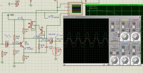
Simulation: 9v supply, input signal 50hz, 2.5v peak
(for both graphics)
Simulation: 9v supply, input signal 50hz, 2.5v peak
(for both graphics)
Attachments


Last edited:
@Ketje
Adding output buffer (your second schematic) is a good idea.
The output signal clips at 2,5v p-p when I add load.
P.s. the Jfet input buffer is with 33k source resistor and it works with 50k load (the volume pot). The simulator does not show clipping as well. It is allready installed.
But the bjt gain stage (the second transistor) clips. It deforms the previous stage signal as well (the red graph).
I am trying to make it with quite large collector resistors and seems it works ok without the output load
Attachments

Not a good idea that RV2, the open loop gain goes down.But the bjt gain stage (the second transistor) clips. It deforms the previous stage signal as well (the red graph).
I am trying to make it with quite large collector resistors and seems it works ok without the output load
To get both sides clip at the same level, play with the value off R16 (now 150k).With that the voltage on the collector Q6 can be adjusted.
Mona
RV2 reduces the gain - I dont know how much boost I need (mby 6 db).
Indeed, playing with R16 results in symetric clip (2,5 v p-p input)
But, simulating with no load shows no clip at almost 3,5 v p-p input.
So, adding output buffer (under fed, 33k collector resistor) might solve the issue, still with a low current draw?
I will try with your extended schematic.
p.p. I have hard time to follow the BJT design procedure - mby the simulator does not take into account the transistor load line, current saturation and so on?
Not sure if the results are real, otherwise looks good 😀.
@Kartapus - the proteus file attached (proteus 8)
Attachments

Last edited:

Is the above a Sziklai pair with some feedback (around the cap)?
Cant figure out the value of R17 (the collector resisor of the PNP transistor)
Cant figure out the value of R17 (the collector resisor of the PNP transistor)
R17 is between the emitter and base of Q6.There is a voltoge on that resistor to make Q6 awake, ~0,6V.Is the above a Sziklai pair with some feedback (around the cap)?
Cant figure out the value of R17 (the collector resistor of the PNP transistor)
So the current for R17 and hence Q5 is 0,6/R17.
Mona
What would u recomend for output current, in order to drive 50 k load?
max half amplitude/ Load R and something over
f.ex. 3.5v/ 50k = 0.07ma
I remember some recomendation of: Zin = 10x Zout
Is 7 times ok? 0.5 mA
You mean peak one side I guess? So it is not 3.5 but 3v/50k = 0.06
10x is 0.6 mA
max half amplitude/ Load R and something over
f.ex. 3.5v/ 50k = 0.07ma
I remember some recomendation of: Zin = 10x Zout
Is 7 times ok? 0.5 mA
Low output Z doesn't mean high drive capability, depends on the bias current.
The ouput level is max ~3Vpeak. With a bass boost of 10x the max input is 300mVpeak (200mVrms).And that 300mV goes for the other frequencies too.
Mona
You mean peak one side I guess? So it is not 3.5 but 3v/50k = 0.06
10x is 0.6 mA
Last edited:
Don't forget the output has to drive the feedback resistors (last schematic R19+RV2) too.That is ~11k//50k=9k.What would u recomend for output current, in order to drive 50 k load?
3Vpeak (not Vpeak-peak) gives 1/3mA.Not much current left to drive something, better use a buffer.
Mona
Don't forget the output has to drive the feedback resistors (last schematic R19+RV2) too.That is ~11k//50k=9k.
3Vpeak (not Vpeak-peak) gives 1/3mA.Not much current left to drive something, better use a buffer.
Mona
I do not understand. If RV2 (also R19) is higher value, there is less current for the output.
If they are lower value, we have both more output current and more load to be driven .... ????
R17 is between the emitter and base of Q6.There is a voltoge on that resistor to make Q6 awake, ~0,6V.
So the current for R17 and hence Q5 is 0,6/R17.
Mona
This is the base current? Shold be in some relation to the output current, via the 'hfe'.
(Ic = Ib * hfe)
But a lot of schematics work without without knowing exact hfe of particular transistor.
Here I do not see any graph, base current vs whatever.
Actually, cant recognize how to use any of these graphs for DC load and finding Q point 🙁
(have some BC559's for the output transistor)
Attachments

I will try it with simulator results for minimum current draw, still not clipping (at least 4 mA, 50k external load, simulated).
Gain is 1 + R19/R18 for the low shelf, 1 for the high shelf.
The -3db point is R19, C15 (high pass, negative feedback).
But R17... the simulator shows the same response in a quite wide range. F.ex 22k - 470k and more.
Dont know what to put there 😀
Gain is 1 + R19/R18 for the low shelf, 1 for the high shelf.
The -3db point is R19, C15 (high pass, negative feedback).
But R17... the simulator shows the same response in a quite wide range. F.ex 22k - 470k and more.
Dont know what to put there 😀
Attachments
Last edited:
Max current draw is: (Vcc/2) / ((R18+R19) || R load)
If we have Vcc 9v, R18 3k3, R19 10k, R load 50k
Boost gain: 1 + 10/3k3 = 4; +12 db. Simulator shows ~11db.
Current draw: 4,5 / ((10+3,3) || 50) = 4,5 / 13,3 || 50 = 4,5 / 10,5 = 0,428 mA. Pretty close to the simulator.
R17 determines base current for the output transistor, but cant figure it from specs.
Simulation shows u can put almost anything
Actually, R17 is not the base current of Q2. The current flows +Vcc - Q2 emmiter - Q2 base.
I dont know what it does and how to calculate it.
All I see is it works on simulator in a wide range of values (~20k - 500k)
Any value suggestion?
I dont know what it does and how to calculate it.
All I see is it works on simulator in a wide range of values (~20k - 500k)
Any value suggestion?
- Home
- Source & Line
- Analog Line Level
- shelving bass boost circuit