Hello, Happy New Year everyone!
A+ quality stuff LC! Congratulations! Awaiting results.
as
I am back into building some SSAs. I couldn't forget its touch...
Thank you Shaan
")
All the best wishes to you too. One of my wishes is to visit amazing India, hopefully wish will be granted some day.

Yes it is touchy indeed.
My HP (high performance) version only looks complex but in real it is very close to the basic SSA circuit. Mosfet driver of BIGBT outputs is a good compromise between performance and VAS insulation so it plays very important role in a simple circuit like this.
Pick one of the "complex" versions and enjoy.
Best regards, Andrej
Hi, happy new year, LC
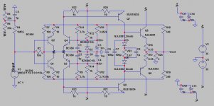
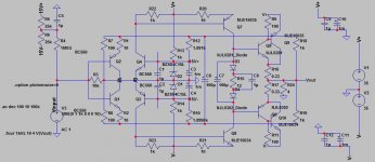
The attached picture is the circuit i'm going to build (ultra low gain), could you help me see any problem/lack in it ? I'm going to construct based on that.
Planning to have 14mA on MJE pairs, and 27mA on NJL pair, is it ok ?
Hi guitar89
This SSA circuit is perfectly functional and can achieve decent distortion levels at low output currents, but if you intend to drive 4 ohm speakers at full swing, than I would suggest you to insert mosfet driver transistor in the output stage. In proposed version output current reverse influence is very high, so all transistors will be dramatically affected. VAS gain transistor is also very important, instead MJE15034/35 I would rather take 2SA1478/2SC3788 or similar high hFE, high fT, TO-126 case transistors and IRF610/9610 for the drivers.
Regards, Andrej
Attachments
Last edited:
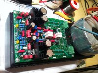
Very professional. I would say world class.
Thanks Nico, greatly appreciated.

It took a lot of effort to design the PCB of exact dimensions according to my plans of how the amp will look at the end. Unintentionally also has, as you've said, "world class" touch hehe.
Regards, Andrej
Attachments
Last edited:
Hi guitar89
This SSA circuit is perfectly functional and can achieve decent distortion levels at low output currents, but if you intend to drive 4 ohm speakers at full swing, than I would suggest you to insert mosfet driver transistor in the output stage. In proposed version output current reverse influence is very high, so all transistors will be dramatically affected. VAS gain transistor is also very important, instead MJE15034/35 I would rather take 2SA1478/2SC3788 or similar high hFE, high fT, TO-126 case transistors and IRF610/9610 for the drivers.
Regards, Andrej
Andrej, nice board you have there ! My creation is such a mess X.x I already built and tested, seems not to my standard(maximum volume) So I configured to higher gain (FBresistor 340 become 680 ohm) and remove the 2k7 resistor, let the VR do the job alone. In the new arrangement, I bias VAS to 8mA, OPS to 15mA. Is it fine ?
Also tested and listened, seems no problem except the heatsink aren't large enough. (I lack of heatsink, so i took one from old computer processor's )
I have a separate heatsink for output and driver. The driver tend to heat up very slow, and the VAS' Iq rise very slow. (about 0.8mA). So as my output's Iq rise slowly from 0.33mA. It takes VAS to heat up to optimum about 1 hours (Iq reach 8mA) and OPS seems heat up fast enough(few minutes) if I play music maximum (computer source) but not VAS.
Is it better to do this way, or put them together ? (then i have to find larger another heatsink)
Anyway, this amplifier is brilliant in term of sound. So i'm thinking to build another one with better VAS and OPS. While now I'm hard to get my hands on different transistors, I'm more focus on arrangement (topology). Have you seen this attached ? I'm not familiar with it but it seems good to me, so hope anyone could guide me
Any good suggestion, I will try my best to get hold of those better transistor ?
Anyway, what is reverse current influence ? Didn't heard this term before.
Attachments
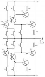
Anyway, this amplifier is brilliant in term of sound. So i'm thinking to build another one with better VAS and OPS. While now I'm hard to get my hands on different transistors, I'm more focus on arrangement (topology). Have you seen this attached ? I'm not familiar with it but it seems good to me, so hope anyone could guide me
Any good suggestion, I will try my best to get hold of those better transistor ?
Anyway, what is reverse current influence ? Didn't heard this term before.
So you've experienced the taste of SSA's sound, nice.
Look, the main reason for VAS temperature to rise so slowly lies in slow thermal response of the VAS transistor/heatsink combination. VAS transistor probably has too large heatsink (big thermal inertia), so it takes so much time to stabilize at certain terminal temperature. Until it gets there, VAS current is slowly changing accordingly to the temperature slope. I suggest you to use smaller heatsink which will allow temperature to stabilize much faster.
Lower part of your output schematic has to be corrected. Emitters are connected correctly, only you have to change Q2 to PNP, Q4 to NPN, Q6 to NPN and Q8 to PNP.
Upper half is correct.
Proposed output sch would work, the only problem I've experienced, because I tested exactly this topology many years ago, is with Q3 and Q4 to be bipolar transistors. Their base currents are added to the emitter currents, thus causing unsymmetrical voltage drop at R5/R9 and R6/R10, resulting in non 50/50 output current (both, quiescent and operational) split between Q5/Q7 and Q6/Q8.
If you replace Q3 and Q4 with mosfets, you will get perfect symmetry between Q5/Q7 and Q6/Q8.
Anyway, what is reverse current influence ? Didn't heard this term before.
I said output current reverse influence not reverse current influence. Big difference. It simply means that the output load current fluctuations/variations strongly affects all previous stages, causing higher percentage of alteration of operational currents value in VAS and input stages than if there would be one more stage present ie. driver transistor (more current gain). Usually we are using the term "VAS current insulation", meaning we are not affecting front-end voltage gain stages (input + VAS), by any means, with output load currents variations. Hopefully I explained it satisfactory.
Last edited:
Hm..... may consider using smaller heatsink, but may overheat ?.... I suggest you to use smaller heatsink which will allow temperature to stabilize much faster.
Lower part of your output schematic has to be corrected. Emitters are connected correctly, only you have to change Q2 to PNP, Q4 to NPN, Q6 to NPN and Q8 to PNP.
Upper half is correct.
Proposed output sch would work, the only problem I've experienced, because I tested exactly this topology many years ago, is with Q3 and Q4 to be bipolar transistors. Their base currents are added to the emitter currents, thus causing unsymmetrical voltage drop at R5/R9 and R6/R10, resulting in non 50/50 output current (both, quiescent and operational) split between Q5/Q7 and Q6/Q8.
If you replace Q3 and Q4 with mosfets, you will get perfect symmetry between Q5/Q7 and Q6/Q8.
It was quite a big mistake in the schematic
Couldn't understand why it affects symmetricity, but leave it alone
Actually I'm fond (more on admire) of IGBT & MOSFET, but couldn't know how to pick them.... (important parameter, characteristic, etc)
I said output current reverse influence not reverse current influence. Big difference. It simply means that the output load current fluctuations/variations strongly affects all previous stages, causing higher percentage of alteration of operational currents value in VAS and input stages than if there would be one more stage present ie. driver transistor (more current gain). Usually we are using the term "VAS current insulation", meaning we are not affecting front-end voltage gain stages (input + VAS), by any means, with output load currents variations. Hopefully I explained it satisfactory.
 Yes, Satisfactory ! I learn about that somewhere, but in that term, just know that it affects VAS lesser (lighter work load).
 Would like to add one, but my current board have no spaces for that Any good arrangement you would suggest for driver/predriver ?
Hm..... may consider using smaller heatsink, but may overheat ?
8 mA VAS current at 50 Vce results in 0,4 W idle power dissipation. That is nothing for MJE15034/35 you are currently using. They could easily handle 0,4 W without any heatsink at all, since they have TO-220 case.
Would like to add one, but my current board have no spaces for that Any good arrangement you would suggest for driver/predriver ?
Standard combinations of pre/drivers: BD139/140 and MJE 15031/15032, MJE340/350 and MJE15034/15035
Suggested: 2SA1478/2SC3788 and 2SA1930/2SC5171
Mine usual: BF471/472 and IRF610/9610
etc.
Last edited:
hm.... since then, should I thermal-couple the VAS ?8 mA VAS current at 50 Vce results in 0,4 W idle power dissipation. That is nothing for MJE15034/35 you are currently using. They could easily handle 0,4 W without any heatsink at all, since they have TO-220 case.
Standard combinations of pre/drivers: BD139/140 and MJE 15031/15032, MJE340/350 and MJE15034/15035
Suggested: 2SA1478/2SC3788 and 2SA1930/2SC5171
Mine usual: BF471/472 and IRF610/9610
etc.
hm..... I guess i will just use my MJE15032/33/34/35 for driver. Could you help me edit the schematic roughly how i'm going to incorporate the driver ?
Thanks Nico, greatly appreciated.
It took a lot of effort to design the PCB of exact dimensions according to my plans of how the amp will look at the end. Unintentionally also has, as you've said, "world class" touch hehe.
Regards, Andrej
Well done board, LC. It looks great on that heatsink
Have you gotten to listening tests for this prototype by now?Well done board, LC. It looks great on that heatsink
Thanks MagicBox
Last days I'm spending most of the time behind computer, preparing some tender documentation, very time consumable. Hopefully I will find some free time next week. Sorry, the job is first on the list and than electronics, although I would rather see the oposite.

P.S. Still, I cheated a little and designed a little sexy PCB in between time.

 Here it is, my little sexy PCB.
er.... LC, last time you said that the design have problem of "output current reverse influence". Could there be any symptom ? I just found that my amplifier have some little issue.
(I) Have high distortion(somewhat like clipping) with high frequency. (not music problem)
Not sure is it clipping, but it is similar with when some amplifier is driven too hard (only high frequency only though)
(II) Not quite compatible with my laptop integrated soundcard. The symptom is (I) increase dramatically(very obvious). The soundcard was no problem with other speaker system.
Previously I was testing with better external soundcard, with better sound, the distortion is less obvious. (sounds like music defect, but actually not)
There can be several reasons for HF distortion or clipping like sounds: too low initial bias current, not enough current gain from all three stages, HF oscillations, bad wireing etc. You certainly have to investigate further the scope image of the output signal to find out the cause of the problem.
huhu, i don't have a scope anyway X.x
But I found out another situation, so I quite have a conclusion.
When I just start it up again the second time, it distort alot even i'm using the external soundcard. Then it is getting better, so I try at laptop's integrated soundcard, result is approx same sound.
So I deduce that it is problem of bias and temperature..... I guess need to let VAS to reach stable temperature first...... Any other way than using thin heatsink ? any other solution ? (If i put starting Iq too high, when it reach optimum temperature, it will be too high temperature for too high bias, becoming too hot)
LC, i'm just thinking that, the bias should be almost ideal (same condition as BE) since the Thermal Track Diode is responsible for the voltage drop, then remove the potentio VR which for bias.
The voltage should be exact enough for just turning on the OPS ? (But in simulation, although the THD is almost same, but the phase and
Just like 1st schematic.
On another side, i'm thinking building another based on different OPS, which is CFP(Sziklai). The another schematic is attached, could you help me to detect anything for compensation or improvement. ?
The posted one is at low gain, but i would like to make it to higher gain. (wanted high performance.
I saw alot said the thermal should stick at driver, instead of output. I was also wondering which category of transistor suit which respective places.(as driver and output device)
Attachments
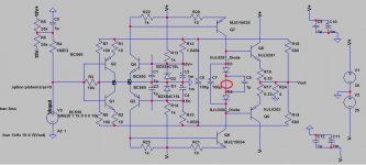
HI guitar89
First sch: the amp would certainly be in a B-class since sensing diodes have lower forward voltage than Vbe. Crossover distortions with underbiased outputs in this sch configuration would dominate the sound. This kind of simple topology is best sounding with more than 150 mA of output's bias current.
Second sch: more adequate way of an output configuration for lower, 4 ohm impedance loads, very strong local feedback with R16,17 in this position. I would rather put them to emitter-rail connection of the outputs. Also lower the value of R9,10 to 33 ohm and certainly change VAS BJTs (predriver) Q7,8 to high performance TO-126 transistor I already previously suggested.
Regards, Andrej
Means that move the R16/17 to output emitter, do there still any resistor between two half ? (I saw some books recommend to put 1 more individual emitter resistor for each transistor at OPS, without moving current configuration.)I would rather put them to emitter-rail connection of the outputs. Also lower the value of R9,10 to 33 ohm and certainly change VAS BJTs (predriver) Q7,8 to high performance TO-126 transistor I already previously suggested.
About the VAS transistor, which should I take ? (I had some selection here)
Thanks Nico, greatly appreciated.
It took a lot of effort to design the PCB of exact dimensions according to my plans of how the amp will look at the end. Unintentionally also has, as you've said, "world class" touch hehe.
Regards, Andrej
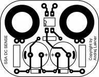
Hi LC!
Great amp
I'm confused, isn't this PCB designed by Alex mm ?
Attachments

Last edited:
- Status
- This old topic is closed. If you want to reopen this topic, contact a moderator using the "Report Post" button.
- Home
- Amplifiers
- Solid State
- Simple Symetrical Amplifier