Yes, you will see the back emf limiting diodes shown on some schematics. They are especially important if there is active current, or IV, limiting fitted to protect the output.
They are wired from Output rail to +ve and from Output rail to -ve. It is better (lower impedance to a fast transient) if they are close to the output devices/pins.
I also use diodes from Power ground to +ve and Power ground to -ve on the PCB. These protect the amplifier and protect the electrolytics from reverse voltage if one is ever daft enough to plug in the PSU incorrectly. I have damaged two amplifiers in my "daft" moments. I have had more daft moments since, but the diodes saved the day, the bulb just lights up.
These 4 diodes can be 1n4002, or higher, to suit the supply voltage you use. I buy by the hundred for a couple of pence each (= 0.08GBP/amplifier)
Last edited:
Yes the diodes are a good desing for that protection, but for this amp i want to keep component count down 🙂, and the fail i described is the ONLY time this amp has "failed", so far im still using my 7294 as shown in the pictures 🙂, time has just kept messing with me so i never completed the 7293, but things are stable now so hopefully ill get to that some dag and make the new thread about the 7293 🙂
................They are especially important if there is active current, or IV, limiting fitted to protect the output...................
The 3886 has active IV protection for the output stage.Y................ but for this amp i want to keep component count down ..................
The output to rail diodes should be considered compulsory.
This is another item that National fail to mention in the datasheet.
The 3886 has active IV protection for the output stage.
The output to rail diodes should be considered compulsory.
This is another item that National fail to mention in the datasheet.
quite right. don't ask me how i know :--))
More stable it is, there's a nicer bootstrap cap hookup, and all 15 pins work. 😀. . . time has just kept messing with me so I never completed the 7293, but things are stable now so hopefully I'll get to that some day and make the new thread about the 7293 🙂
So, I think you're going to enjoy this.
hehe i was refering to my life 😛, but yes some day i will look forward to the 93, also for everybody reading this thread there is a facebook page for it also
https://www.facebook.com/groups/760434413975466/
https://www.facebook.com/groups/760434413975466/
Hello,
I've a question about the TDA7294 amplifier.
What's the input voltage allowed on this amplifier, before it distort the signal?
I'm powering it at +-35V, driving an 8ohm speaker.
Actually I've a 10x preamp, it means as example that a 250Hz sine @ 100mV get transformed in a 1V sine, but i suppose i can reach a higher voltage to have a little more volume.
Thanks!
p.s. sorry for my poor electronics 🙂
it depends on what gain you have set for the chipamp.
if it's 26x then the chipamp will clip at somewhat less than 1 vrms input using a +/- 35V PSU.
see the datasheet.
if it's 26x then the chipamp will clip at somewhat less than 1 vrms input using a +/- 35V PSU.
see the datasheet.
it depends on what gain you have set for the chipamp.
if it's 26x then the chipamp will clip at somewhat less than 1 vrms input using a +/- 35V PSU.
see the datasheet.
Thank you, unfortunately i'm not able to read datasheet for this clipping value. Where did you find the 1vrms clip information?
Attached the schematic i'm using. It's for a bass guitar amp.
The circuit is almost the typical application circuit of the ST datasheet. So using that r2 and r3 values, is the gain the 30db value that i read in page 5 of the ST datasheet "(CLOSED LOOP GAIN SET TO 30dB (**)"?
Thanks again!
Attachments

i wish i had the time to go through that schematic with you. perhaps others can chime in. a couple examples of obvious problems:
1. because the second stage is inverting, the tone stack is part of the feedback loop area in that stage. not a good thing.
2. the bootstrap cap and the dc block cap in the chipamp stage are too small for a bass amp.
3. the rails need bypassing in every stage of the amp.
1. because the second stage is inverting, the tone stack is part of the feedback loop area in that stage. not a good thing.
2. the bootstrap cap and the dc block cap in the chipamp stage are too small for a bass amp.
3. the rails need bypassing in every stage of the amp.
Hello,
I've a question about the TDA7294 amplifier.
What's the input voltage allowed on this amplifier, before it distort the signal?
I'm powering it at +-35V, driving an 8ohm speaker.
Actually I've a 10x preamp, it means as example that a 250Hz sine @ 100mV get transformed in a 1V sine, but i suppose i can reach a higher voltage to have a little more volume.
Thanks!
p.s. sorry for my poor electronics 🙂
You are asking the wrong question.Thank you, unfortunately i'm not able to read datasheet for this clipping value. Where did you find the 1vrms clip information?
Attached the schematic i'm using. It's for a bass guitar amp.
The circuit is almost the typical application circuit of the ST datasheet. So using that r2 and r3 values, is the gain the 30db value that i read in page 5 of the ST datasheet "(CLOSED LOOP GAIN SET TO 30dB (**)"?
Thanks again!
What is the maximum output signal when the supplies are +-35Vdc?
The maximum output signal with no load attached (or a very high impedance load, like 10k resistor) will be ~1volt less than the supply rails, i.e. 34Vpk.
With a typical 8r0 load attached the maximum output voltage will be ~3volts less than the supply rails, i.e. 32Vpk.
32Vpk converts to 22.6Vac sinewave.
For an 8ohms speaker load, that is equivalent to 64W
Now YOU decide what amplifier gain YOU want to adopt.
Apply that to the OUTPUT signal to find the maximum INPUT signal @ the input pins.
Say you choose 20times (+26dB), then you get 1.13Vac
The RF filter at the input will attenuate the input very slightly. Thus you need a tiny bit more. Try applying 0.95 as the passband attenuation to get an input signal at the amplifier input socket of around 1.2Vac, or 1200mVac
Last edited:
i wish i had the time to go through that schematic with you. perhaps others can chime in. a couple examples of obvious problems:
1. because the second stage is inverting, the tone stack is part of the feedback loop area in that stage. not a good thing.
2. the bootstrap cap and the dc block cap in the chipamp stage are too small for a bass amp.
3. the rails need bypassing in every stage of the amp.
I take "inspiration" for this circuit from the "SWR Workingman's 10" and the "Ampeg BA115" circuit (can not post the circuit here, but it can be found online).
Also my analog electronics knowledge unfortunately is not so good. So i hope you forgive my dumb questions.
1. i need to study it a little more to understand why 🙂
2. C1 (47uf), and C19 (10uf) should be better?
3. i should add a caps next to the opamp power input?
Thanks AndrewT.
As you can read, as i tell sfthurber, i hope you forgive my dumb questions.
As you can read, as i tell sfthurber, i hope you forgive my dumb questions.
I don't get it where did you read in the datasheet the ~1volt value for 34Vpk and how do you compute the value for a 8ohm load.The maximum output signal with no load attached (or a very high impedance load, like 10k resistor) will be ~1volt less than the supply rails, i.e. 34Vpk.
With a typical 8r0 load attached the maximum output voltage will be ~3volts less than the supply rails, i.e. 32Vpk.
Again, i don't know the math behind this 🙁For an 8ohms speaker load, that is equivalent to 64W
Do you mean the C18 caps filter?Try applying 0.95 as the passband attenuation to get an input signal at the amplifier input socket of around 1.2Vac, or 1200mVac
I don't use any of the TDA chipamps and don't have the datasheets to hand.
Maybe they don't give as much information as the National chipamp datasheets, but even National choose to publish the information that LOOKS good to their potential customers and deliberately hide useful information, it were to put their product in a poor light.
A couple of examples:
Virtually all their data is for resistive dummy loads and almost none for reactive loads typical of a speaker.
Virtually all their data is for Tc=25°C, even though most chipamps operate with Tc >>25°C
You will need to read between the lines to extract the TDA information and that will require you to learn how to read what they choose to show and how to interpret what they don't show.
Power
P=IV=I²R=V²/R
and all the converted versions, for non constant DC voltage and current.
C18=47pF in post409?
Don' know what capacitor is there for.
Maybe they don't give as much information as the National chipamp datasheets, but even National choose to publish the information that LOOKS good to their potential customers and deliberately hide useful information, it were to put their product in a poor light.
A couple of examples:
Virtually all their data is for resistive dummy loads and almost none for reactive loads typical of a speaker.
Virtually all their data is for Tc=25°C, even though most chipamps operate with Tc >>25°C
You will need to read between the lines to extract the TDA information and that will require you to learn how to read what they choose to show and how to interpret what they don't show.
Power
P=IV=I²R=V²/R
and all the converted versions, for non constant DC voltage and current.
which schematic/which post?Do you mean the C18 caps filter?
C18=47pF in post409?
Don' know what capacitor is there for.
Last edited:
That's why is said my questions are dumb 🙁P=IV=I²R=V²/R
Yes, i thought it was the RF filter you are speaking of, but it was not.C18=47pF in post409?
Anyway, thanks for help!
Charmers for ST include TDA7265 (smaller room), TDA7265B (larger room) TDA7293 (great room/pub/party) as well more specialized purpose parts, such as the TDA7297 (car/econofi), TDA2009 (old fashioned singleton input sound, and good for nearfield purpose amp on regulated power). And, there's a lot more.I don't use any of the TDA chipamps and don't have the datasheets to hand.
The datasheet schematics may be at least as uninformative/counterproductive as expected for chip amplifiers (you'll get only the usual generic schema even if the chip couldn't or shouldn't do it); however, the text and chart portions of the datasheet are pretty good.
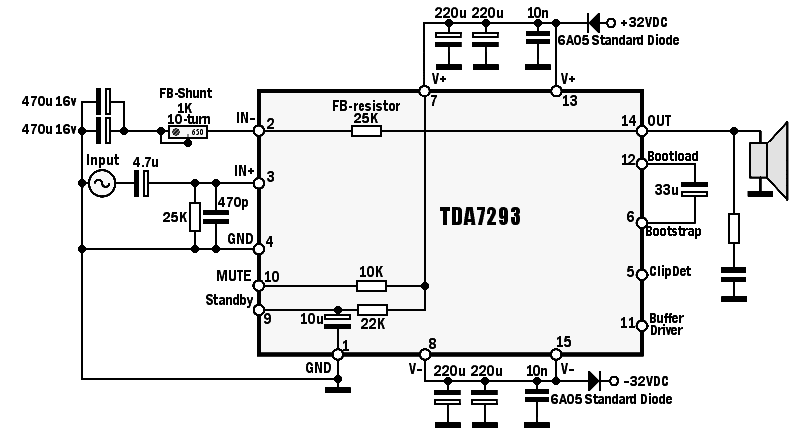
Found this one on the net
warm regards
andrew lebon😀
dear plz share pcb or tell me the source
thanks regard
These are 0,15R resistors. See the schematic in the previous page.
I used the pcb design by kebbz, provided by him on page 9.
The board i used, was just a bit smaller than needed for this design, so i had to run some tracks on top of the board.
I'm currently under the impression that the amp is underpowered, based on the theoretical capabilities.
I don't know what melted the woofer though🙁
plz pcb in pdf thanks
dear plz share pcb or tell me the source
thanks regard
plz share me yr pcb thanks
- Home
- Amplifiers
- Chip Amps
- TDA7294 + Power Transistors AMP (TDA7293 to come also)