Maybe my next big amp will use those beastly hockey pucks. Tempted to build an XA25 derivative, or even a second F6 with a set of IXFK 140N20P devices (TO-264 style).
Ixys has a new n channel part "IXFH94N30P3" that according to their spice model, except for a few tenths of a volt of offset, it has the same transfer curve as the IXTK40P50P. I don"t know how accurate their models are.
The last step I did in Ltspice might not be done correctly in order to line up the curves. So, the curves might not line up as shown above. I had to flip the p channel curve, that was easy, but I might not have moved it back properly to match them up. I hope someone with better skills will take a look at this. They sill might be a good match. I have been getting very good distortion numbers using them in simulations.
If you're mosfets are thermally drifting more than you're happy with, I have a very simple idea to improve it.
If it's not an issue you're irritated by, then no worries.
This would be an interesting idea to have in my toolbox for the next big amp. The bias current in my F6 does slowly drift upward as it approaches thermal equilibrium, but this isn’t really a problem, so much as something that I need to consider.
You just might be petrified as how compact my amps are. Both my F6 and Aleph J are housed inside a 3.5U, 400mm deep chassis. The trick is to use the entire outside of the case as the heat sink.I'm chicken , so I wouldn't dare to use those biguns without tight Iq control
")
I am curious how one might implement more control over Iq in an F6-like circuit, while keeping the best qualities of the F6.
It really is wonderful to wake up in the morning and listen to an amplifier that has been so nicely dialed-in. I'm tempted to drop some green thread-locking compound onto the screws in the top plate to discourage further tampering. I left in the 120Ω gate stoppers, though I could see a case for 100Ω values here. I will save the 75, 47 and 22 Ohm values for more beastly output stages.
The SLB power supplies do provide a soft current limit, as they don't regulate output voltage, just remove ripple. Last I checked, I was getting about 2mV of ripple on the output, but that was before I added the 24mF bulk caps. I do find it important to have real capacitance on the power rails. Cap multipliers work effectively to reduce ripple, but don't supply real current to an output stage or introduce a real dominant low-frequency pole into the system. The ripple reduction really does work though, including times when the furnace blower or refrigerator kick on. Setting bias current has certainly been easier with better immunity from dirty AC power.
I'm pleased with the results of using higher transconductance Mosfets, as well as lower source resistance in the output stage. I'm also glad I used a diamond buffer to replace the simple JFet input buffer. I'm hearing some similarity between this amp and my M2x when fitted with the Austin IPS, and that's a happy thing.
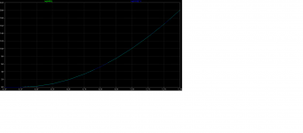
I ran the transfer curves separately in ltspice for each off those ixys parts and took some voltage and current points off the graphs starting at 1 amp. It shows somewhat how well they match. It also shows that the method I did in the above post does not work.
n type p type
4.513 1.000 4.713 1.000
4.613 2.116 4.813 2.107
4.713 3.634 4.913 3.600
4.813 5.543 5.013 5.456
4.913 7.834 5.113 7.662
5.213 16.898 5.413 16.163
n type p type
4.513 1.000 4.713 1.000
4.613 2.116 4.813 2.107
4.713 3.634 4.913 3.600
4.813 5.543 5.013 5.456
4.913 7.834 5.113 7.662
5.213 16.898 5.413 16.163
If you're mosfets are thermally drifting more than you're happy with, I have a very simple idea to improve it.
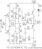
Worth noting from the schematic that if the wiper of P3 is pointed to the
Source of Q1, then the output stage is running Common Source without
degeneration at AC frequencies because the transformer is driving the
Gate to Source junctions.
This being the case, R1 and R2 can be higher values without significant
change in performance or sound, so it's easy to fix bias drift that way.
Attachments
Worth noting from the schematic that if the wiper of P3 is pointed to the
Source of Q1, then the output stage is running Common Source without
degeneration at AC frequencies because the transformer is driving the
Gate to Source junctions.
This being the case, R1 and R2 can be higher values without significant
change in performance or sound, so it's easy to fix bias drift that way.
That is very true.
It is the most satisfying thing to see you post new revised circuits.
Papa oi
I had a new idea not necessarily for this circuit (but it would still work), I would like to discuss with you. It's dumb simple.
Last edited:
I am curious how one might implement more control over Iq in an F6-like circuit, while keeping the best qualities of the F6.
It is absolutely dumb simple.
It's so dumb simple I am punching myself for not thinking of it earlier.
I will be testing it out.
I'm hoping that a simple solution is equally simple to write about...
I haven't applied the threadlocker to my case screws yet, so I might still be convinced to remove the top plate. It would be nice to have an amp that was able to reach a stable temperature in a shorter period of time. Part of the issue is that with cold heatsinks, the initial bias current is pretty low, maybe 1.2 A. There is a slow increase in bias current as the heatsink temperature slowly rises. The final results sound very good, but require some patience.
I haven't applied the threadlocker to my case screws yet, so I might still be convinced to remove the top plate.
It would be nice to have an amp that was able to reach a stable temperature in a shorter period of time. Part of the issue is that with cold heatsinks, the initial bias current is pretty low, maybe 1.2 A. There is a slow increase in bias current as the heatsink temperature slowly rises. The final results sound very good, but require some patience.
Last edited:
I'm hoping that a simple solution is equally simple to write about...
I haven't applied the threadlocker to my case screws yet, so I might still be convinced to remove the top plate.
The DEFiSIT I am testing has this behavior. Both devices have a positive tempco. The initial bias has to be quite low to achieve low offset at high bias at 50 deg C heatsink temp.
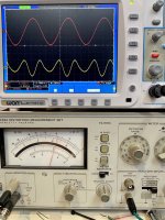
My curiosity finally got the better of me, and my F6 was put back on the test bench, hooked up to the analyzer. The configuration remains as described in post #1893
The attachment shows the THD reading at 5 Watts output into an 8 Ohm load. Compared with the previous "too much of a good thing," this is showing 0.21%. When measured at a more typical 1 Watt out, THD drops down to a more respectable 0.088%. So, not bad for a case of deliberate coloration. I could try dropping the C1 attachment resistance a bit lower, perhaps to 0.05Ω, as suggested by 2 picoDumbs, but that would probably require better matching of the resistors and the Mosfets themselves in order to be meaningful. Not sure if I'm up for that just yet. One more data point: measured gain is 15.6 dB
The amp is still a pleasure to listen to, and at the same time quite revealing of the choices made in the recording studio. I'm off on another short trip for the next week, so I'll see how I feel about it after I get back.
Attachments
Last edited:
I'm hoping that a simple solution is equally simple to write about...
I haven't applied the threadlocker to my case screws yet, so I might still be convinced to remove the top plate.
Please be patient.
I really want to test it first, so I can give you a quantitative figure for the kind of improvement you can expect to get.
I have ordered the parts, I should have them in a week.
This is my first amplifier build but got it completed. Having some trouble understanding the baising and offset process. I used a 6.8v / 1.3 watt zener diode for the build. If it helps the sound coming out of the amplifier is distorted. The best way to describe it is as if it had a faulty ground but I have meticulously reviewed all connections and grounds. Also have no heat coming off of the heat sinks as other have described. My output voltage at the PSU is 25.7V so I think I'm good as far as power side of the amp goes.
For the bias I am reading with a DC volt meter across R2 (one meter lead on each side of the resistor)on the PCB audio board I get zero volts. I saw some other posts and so tried measuring from one lead on R2 (Source resistor) to ground on the audio PCB board and got 25.63 volts adjusting P2 doesn't seem to do anything.
For offset I measured at the speaker terminal output with the connector looped. There I am reading .010V.
So not sure I am reading the values for the bias or the offset at the correct test points nor am I able to adjust with what I am doing. Any insight would be extremely helpful
Regards
Bob
- Home
- Amplifiers
- Pass Labs
- The diyAudio Firstwatt F6