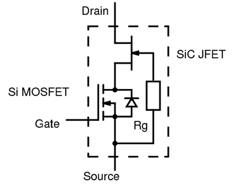
The future of Silicon Carbide is LV Si MOSFET cascoded with HV SiC JFET (in same package).
Recommended reading:
Power Systems Design (PSD) Information to Power Your Designs
The problem with economic speculators funding technological R&D:
Everything they fund becomes flawed and perishable. Speculation is only for perishables.
This phenomena has to do with the type of human relationship between researchers and fund providers. Speculators want to be on top of "blood" hierarchy. This biologically forces researchers to use the creativity filters of speculators. As a result, the product reflects, as flaws, one by one, all "sins of origin" of funding speculators.
This is also the story of the technological "bubble burst" under development.
Last edited:
also used interestingly in single switch resonant forward converters:
http://www.uni-kassel.de/upress/online/frei/978-3-89958-302-1.volltext.frei.pdf
looks a bit like classE
http://www.uni-kassel.de/upress/online/frei/978-3-89958-302-1.volltext.frei.pdf
looks a bit like classE
Thanks. Interesting paper.
The information comparing semiconductor types is good.
Converter discussion includes the infamous "phase-shifted full-bridge", this is an old invention under pressure of brok€r$, to sell more high-voltage slow-body-diode silicon MOSFET, an inherently sub-optimal device for that application. But the application is also sub-optimally made for the sub-optimal device (in other words, it will become obsolete, as old HV MOSFET become too).
Converter discussion has mistakes in half bridge figures (what a coincidence!). It seems the author had not experienced enough with circuits prone to cross-conduction.
"MOSFET with SiC JFET cascode" as switch has the least advantage for the type of test converter proposed (resonant reset forward, yes, it resembles class E RF amplifier). MOSFET and IGBT performs equally well. Most of the advantage of the new technology is for hard switching. (I suppose that student was irrationally sponsored by his family, voiding 50% of competitiveness.)
The prototypes and waveforms look dirty. That student would have worked better in association with someone with expertise in SMPS.
Last edited:
. The team also evaluated super-junction transistors, although unexplained failures of prototypes undermined confidence in the robustness of the body diodes.
This is the second time I have heard about the unpredictable failure mode happening in using super junction MOSFETs .
Evita,
What do you think, the link shared by you says engineers don't have confidence in super junction MOSFETs.
Does anyone understand this part: "Because most of the power is dissipated in the JFET die, the temperature capability is defined by that of the SiC technology. Theoretically, this is 250°C, although package limitations impose a practical maximum of 175-200°C"?
I'd say you still need to keep the temperature of the silicon part down to something it can survive, no matter whether it dissipates all or just a small part of the power.
I'd say you still need to keep the temperature of the silicon part down to something it can survive, no matter whether it dissipates all or just a small part of the power.
What they mean by random "super-junction body-diode failures" is that a too wide spread in body-diode strength is obtained from process.
The silicon MOSFET concept itself is sub-optimal at high voltage. The drift layer required is too thick. It is fat just for achieving voltage blocking, not for achieving surprising Rds-on or body diode Qrr figures. Silicon carbide requires only 1/10th of drift layer thickness.
On the other hand, growing the metal oxide layer for gate on silicon carbide is far more costly than growing same layer for gate on silicon.
These are the 2 factors against plain silicon carbide semiconductors (and in favor of compound Si-MOSFET/SiC-JFET). Who had the idea? How much money was wasted? Why so much advertising for something sub-optimal?
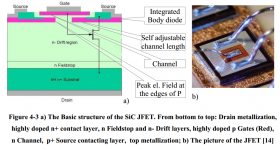
A figure showing die structure is attached (taken from thesis shared in post #2).
The silicon MOSFET concept itself is sub-optimal at high voltage. The drift layer required is too thick. It is fat just for achieving voltage blocking, not for achieving surprising Rds-on or body diode Qrr figures. Silicon carbide requires only 1/10th of drift layer thickness.
On the other hand, growing the metal oxide layer for gate on silicon carbide is far more costly than growing same layer for gate on silicon.
These are the 2 factors against plain silicon carbide semiconductors (and in favor of compound Si-MOSFET/SiC-JFET). Who had the idea? How much money was wasted? Why so much advertising for something sub-optimal?
A figure showing die structure is attached (taken from thesis shared in post #2).
Attachments
Does anyone understand this part: "Because most of the power is dissipated in the JFET die, the temperature capability is defined by that of the SiC technology. Theoretically, this is 250°C, although package limitations impose a practical maximum of 175-200°C"?
I'd say you still need to keep the temperature of the silicon part down to something it can survive, no matter whether it dissipates all or just a small part of the power.
In semiconductors the failure mode at high dissipation is the generation of "hot spots", capabilities of materials are locally exceeded. This happens within the region of the die that is heating itself. The regions of the die being passively heated are under less stress.
Imagine a fuse. You can externally heat a fuse close to melting temperature and you will still be in control. This is not true when the heat comes from dissipation in fusing element, soon there is a no-return point.
The future of Silicon Carbide is LV Si MOSFET cascoded with HV SiC JFET (in same package).
Recommended reading:
Power Systems Design (PSD) Information to Power Your Designs
The problem with economic speculators funding technological R&D:
Everything they fund becomes flawed and perishable. Speculation is only for perishables.
This phenomena has to do with the type of human relationship between researchers and fund providers. Speculators want to be on top of "blood" hierarchy. This biologically forces researchers to use the creativity filters of speculators. As a result, the product reflects, as flaws, one by one, all "sins of origin" of funding speculators.
This is also the story of the technological "bubble burst" under development.
Thanks for the info. Will use'm in my Class aP amplifiers hobby to mimic push-pull vac tubes ones.
Best
Anton
Does anyone understand this part: "Because most of the power is dissipated in the JFET die, the temperature capability is defined by that of the SiC technology. Theoretically, this is 250°C, although package limitations impose a practical maximum of 175-200°C"?
I'd say you still need to keep the temperature of the silicon part down to something it can survive, no matter whether it dissipates all or just a small part of the power.
Silicon devices can be production qualified to operate way up the regular 150 degrees specified for power devices. It's all about derating the power dissipation with temperature and about avoiding thermal avalanche, both less of an issue at low power dissipation. Check out this op amp qualified at 210 degrees http://www.ti.com/lit/ds/symlink/opa820-ht.pdf (and yes, I can vouch it works just fine there, and with a healthy margin, in fact a prototype blew at an estimated silicon temperature of over 250 degrees). I would though not expect such power devices to be available in popular plastic cases, but more likely in flip-chip, factory solder ball-ed (like the OPA820 mentioned above).
There are no physical changes in a silicon structure below some 500 degrees (metallization/contacts are the first to surrender, at least in cheap processes). 200 degrees for the storage temperature is usually imposed to avoid thermo-mechanical stresses in the chip assembly that can crack the silicon and/or wire bonds. Once again, popular plastic packages are not an option at these temperatures.
GaN is for RF, among the most complex to produce, but brokers may tell otherwise.
A 2 inch epitaxial GaN wafer currently costs well over $1000/pc (prices are falling quickly, though, since there's an over supply of Gan since the demise of the GaN lasers). A 2 inch wafer is home for about 50 power devices with any decent transconductance.
4H and 6H n-type, on-axis 4 inch SiC wafers are currently about half that price. Given the fact that GaN and SiC have about the same majority carrier mobility, the net result is an almost x10 higher cost for the initial material, for GaN device.
This may change, GaN devices may eventually win the race, but some break through are still required.
Thanks for tech feedback.
Just considering the availability of Gallium, compared to Silicon and Carbon, it's clear that GaN is never going to win anything for the sort of equipment that is of common use among worlds population.
The exponential growth in USA economy is simulated to push prices down with time. This method was already discarded at other continents. It will be discarded in USA too. In science this is called expectation bias.
Still the very low gate charge for GAN is attractive. I did an active rectifier at 6.78Mhz for a medical implant , where device heating is limited to 2Kelvin (2degrC). that one was far more efficient than schottky rectification at larger currents as the gate drive power was relatively small .
Amazing application!! That's battery-powered bio-friendly miniature RF.
I think GaN is not going to be available in TO-220 packages, due to the fact that most applications are RF.
On the other hand, self-oscillating class-D amplifiers can be made to switch at just 200~100Khz while high power is being delivered. A little amplifier thing with warm heatsink can be pumping tons of bass (or clean mids and highs) to a dancing and loving crowd, just with 150~300V silicon MOSFET.
Problem in this field, with newer fancy transistor technologies that want to go behind TO-220, is thermal cycling. Due to continuously fluctuating audio power demand (120 beats per minute is 2Hz) some thermal mass soldered directly to transistor die is required, or chip and bonding wires age quickly (though some too-simple brands bet for that). High thermal contact surface is needed to, as thermoconductive elastomer pads are almost always used, contributing ~1C/W (TO-220 size) to overall thermal resistance. It is not reliable to go smaller than TO-220 for high power audio.
Problem was resolved by adopting SMD, flip chip derived structures. No bonding wires in these structures, they are an enhancement of the BGA style configuration. Check out http://www.ti.com/lit/ds/symlink/csd19532q5b.pdf
GaN has another disadvantage, it has a much lower thermal conductivity compared to SiC. That’s a net disadvantage at high power.
GaN has another disadvantage, it has a much lower thermal conductivity compared to SiC. That’s a net disadvantage at high power.
Amazing application!! That's battery-powered bio-friendly miniature RF.
I think GaN is not going to be available in TO-220 packages, due to the fact that most applications are RF.
On the other hand, self-oscillating class-D amplifiers can be made to switch at just 200~100Khz while high power is being delivered. A little amplifier thing with warm heatsink can be pumping tons of bass (or clean mids and highs) to a dancing and loving crowd, just with 150~300V silicon MOSFET.
Problem in this field, with newer fancy transistor technologies that want to go behind TO-220, is thermal cycling. Due to continuously fluctuating audio power demand (120 beats per minute is 2Hz) some thermal mass soldered directly to transistor die is required, or chip and bonding wires age quickly (though some too-simple brands bet for that). High thermal contact surface is needed to, as thermoconductive elastomer pads are almost always used, contributing ~1C/W (TO-220 size) to overall thermal resistance. It is not reliable to go smaller than TO-220 for high power audio.
for implantables RF is the only solution for communication and powering. we cannot safely keep a wire sticking out of the skin. most of the other RF stuff is luxury or comfort. why opening you car at 3m distance while you need to be at the door to stick a key in anyway ?
Anyway GaN for the 6.78MHz classD transmitter is different than using MOS. due to the very low gate resistance the gate capacitance is resonating against any sort of inductance in the gate circuit, like the leakage inductance of the gate drive transformer or PCB trace. a gate series resistor is always needed. but driving the GaN gate can be done using a single CMOS buffer.
Problem was resolved by adopting SMD, flip chip derived structures. No bonding wires in these structures, they are an enhancement of the BGA style configuration. Check out http://www.ti.com/lit/ds/symlink/csd19532q5b.pdf
GaN has another disadvantage, it has a much lower thermal conductivity compared to SiC. That’s a net disadvantage at high power.
Flip chip solutions have less interconnect inductance, but more parasitic capacitance everywhere. You still end up with frequency limitations in "50 ohm" systems. Different ones, which are harder to model. Fast 2.5D EM simulators don't work, and you have to use HFSS fior the whole thing. Be prepared for some head banging, and your computer sitting being a paperweight while the little circle sits and spins for a day or so waiting on each solution.
"GaN" is actuallly a thin epi, grown on SiC wafers. Thermal conductivity is quite high, and devices are typically thermally limited by their surroundings. The devices have plenty of fleas and ticks, and if you design in it long enough you'll end up with a case of Lyme disease. Or at least a headache or two.
This was not about frequency response, but about thermal stress at high temperature. Wire bonds are among the first to give up under thermal cycling, so flip chip is the method of choice. It also helps with the Rth between the chip and the substrate.
Epitaxial GaN on SiC is only one of the options for building GaN devices. While it certinly helps with the poor GaN thermal conductivity, the lattice mismatch between SiC and GaN leads to poor crystal properties and as a result to poor device properties. This is one of the reasons why I was saying a breakthrough is required to improve GaN devices, to make them compatible in cost and performance with SiC devices (in the SiC frequency range). I don't think GaN devices will push SiC devices out of the market anytime soon (if ever).
Epitaxial GaN on SiC is only one of the options for building GaN devices. While it certinly helps with the poor GaN thermal conductivity, the lattice mismatch between SiC and GaN leads to poor crystal properties and as a result to poor device properties. This is one of the reasons why I was saying a breakthrough is required to improve GaN devices, to make them compatible in cost and performance with SiC devices (in the SiC frequency range). I don't think GaN devices will push SiC devices out of the market anytime soon (if ever).
- Status
- Not open for further replies.
- Home
- Amplifiers
- Class D
- The future of Silicon Carbide is not in SiC MOSFET, hardly in SiC diodes...