Syn08 (Ovidiu) said this about implementing an Auto Bias loop here:
Well, there's the challenge. A wideband non switching Auto Bias amplifier circuit that works, doesn't oscillate and blow up, and is not too complex.
To start this thread I'll post some of my findings from simulations of the LT1166 Auto Bias IC, as well as Class-i and Edmond's AutoBias2.
Feel free to post any of your ideas and simulations.
And if anyone has built a successful amplifier using an auto bias circuit then we'd love to hear how you did it, etc.
Cheers, Ian
-------------
Edit: Post summary (Edit: most recent first):
Post 303 Shows 3D views of a PCB for Post 302 circuit (now called Topology 4).
Post 302 The LT1223 again but now driving MOSFETs to demonstrate the autobias loop allows plug-in interchange of BJT's and MOSFETs. Interestingly, the MOSFET's achieve similar high BW with less drive current so 2 pair instead of 5 pair TO-92's can be used.
Post 301 The previous LT1223 CFB opamp with a CFP autobias loop is OK for 16MHz(tbc) without the CFP output stage, instead the discrete HV booster is paralleled for 50mA drive to the power transistors with a +/-9V auxiliary supply.
Post 300 The previous CFP BJT autobias loop is OK for 4MHz(tbc) with a LV LT1223 100MHz CFA with a discrete voltage booster giving low distortion.
Post 295 Bridge and current drive is easy with a HV opamp, where one load terminal is tied to input common (grounded bridge) with a floating PS.
Post 291 Current drive with a HV opamp is very easy using a resistor in series with the loads cold-side for feedback to the opamps inverting input node.
Post 287 CFP BJT autobias loop is OK for 100kHz with a 33 Ohm base pull-up to 9V. Allows a low input current (1mA) drive using a HV opamp (OPA455) with a split rail standard power supply.
Post 282 Only THT with current drive for 4 ohms suggested by Pawel.
Post 281 Current drive version for 200W into 4 ohm, Rout 500 ohms and 0.02% at 1W. Uses 2x OPA1656 LV 100mA opamp drivers.
Post 277 Class-G bridge 800W 4R using 4 slices per side for 20A peaks. Idle dissipation is reduced using Class-G plus McPherson's dissipation diverter.
Post 274 Bridge version for 400W 8R is DC input and DC output. Usescapacitance multiplier with McPherson's dissipation diverter.
Post 271 Mark Johnson query: What if the output capacitor divider capsare not exactly the same? Answer: the voltages equalise quickly due to the amps low output resistance.
Post 269 Power supply circuit to check startup with no dc blocking capacitor. Simulation shows no startup or shutdown transient to the loudspeaker.
Post 267 Input stage level shift with no dc blocking input capacitor.Uses an opamp with a -5V rail and a mirror input stage level shifterwith no signal.
Post 266 simulation using ZXT757 and ZXT857 300V complimentary pair for input stage level shift. Bias trimming calculation for output centering.
Post 257 simulation using a level shift input stage rather than a isolation transformer, allowing a standard non-floating power supply.
Post 256 mr_jj pointed out that Kenpeter back in 2010 had placed a resistor across the sensing diodes between the emitters of the power transistors to make it non-switching Class-AB! My hat is off to Kenpeter. I mention my independent finding in Post 202. The Dadson's circuit found in Post 44 here from his AES Oct 1980 article shows the same autobias sensing diode topology using a Rush spreader arrangement but with Darlington power transistors, but no resistor across the sensing diodes.
Post 254 Bench test using thean OPA1656 100mA opamp to drive power transistors with autobias without discrete driver transistors.
Post 244 Bench tests of a single channel amplifier shows -60dB THD using MUR1615 diodes and biased at 250mA. F-3dB is slightly over 100kHz.
Post 243 Shinichi Kamijo "simple TL bias" circuit is similar topology to my autobias but with a follower output stage and a non-floating power supply.
Post 235 Bridge version bench test. Two floating power supply amps on one supply, where one amp uses a small transformer to isolate the input signal.
Post 222 Tutorial on the floating power supply transconductance autobias output stage. More in Post 245 and Post 251.
Post 220 Using MUR1615 TO-220 power diodes instead of Schottky diodes gives excellent linearity. Bias can be trimmed by two resistors to 9V rail instead of two CCS's (simpler and less error prone).
Post 215 Using MJE3055 TO-220 as diodes instead of Schottky diodes.
Post 210 thru Post 214, Post 217-219. Option of using many (8-10) 1A silicon diodes in parallel per side instead of Schottky diodes so no need for a bias trim pot.
Post 205 FDC6321 CMOS stage allows high current drive without a CFP output stage.
Post 203 A prototype PCB allows stacking of up to slices (3 pair of output transistors).
Post 202 Using a HCU04 CMOS input stage with a CFP output transistors so only 1mA is needed to drive the autobias transistors. The CMOS input stage provides some gain and soft clipping and the option of thermal-SOA protection by dynamically limiting the clip level (more in Post 204). Introduced R13 across the power diodes to provides the keep-on current of 18mA in Q1 and Q2 - even when clipping. Eureka!!
-------------------------
Edit Feb 2025. Overview of development: Toward a Wideband Non-Switching Auto Bias amplifier
The challenge! “A wideband non switching auto bias amplifier circuitthat works, doesn't oscillate and blow up, and is not too complex”.Post1 aim 29 July 2021 by IanHegglun.
" I haven't see a solid non switching full solution for the entire audio band, but only partial improvements over the standard solution of an acceleration cap (100nF, in your case), which is not a solution for non switching, but only a bandaid to limit the effect of the crossover mess.
Part of this lack of solutions is of course keeping the complexity within reasonable limits; Edmond's solution mentioned above, in despite of it's stability issues, is already a rather complex circuit, and I don't think anything simpler could be designed and successfully implemented."
Well, there's the challenge. A wideband non switching Auto Bias amplifier circuit that works, doesn't oscillate and blow up, and is not too complex.
To start this thread I'll post some of my findings from simulations of the LT1166 Auto Bias IC, as well as Class-i and Edmond's AutoBias2.
Feel free to post any of your ideas and simulations.
And if anyone has built a successful amplifier using an auto bias circuit then we'd love to hear how you did it, etc.
Cheers, Ian
-------------
Edit: Post summary (Edit: most recent first):
Post 303 Shows 3D views of a PCB for Post 302 circuit (now called Topology 4).
Post 302 The LT1223 again but now driving MOSFETs to demonstrate the autobias loop allows plug-in interchange of BJT's and MOSFETs. Interestingly, the MOSFET's achieve similar high BW with less drive current so 2 pair instead of 5 pair TO-92's can be used.
Post 301 The previous LT1223 CFB opamp with a CFP autobias loop is OK for 16MHz(tbc) without the CFP output stage, instead the discrete HV booster is paralleled for 50mA drive to the power transistors with a +/-9V auxiliary supply.
Post 300 The previous CFP BJT autobias loop is OK for 4MHz(tbc) with a LV LT1223 100MHz CFA with a discrete voltage booster giving low distortion.
Post 295 Bridge and current drive is easy with a HV opamp, where one load terminal is tied to input common (grounded bridge) with a floating PS.
Post 291 Current drive with a HV opamp is very easy using a resistor in series with the loads cold-side for feedback to the opamps inverting input node.
Post 287 CFP BJT autobias loop is OK for 100kHz with a 33 Ohm base pull-up to 9V. Allows a low input current (1mA) drive using a HV opamp (OPA455) with a split rail standard power supply.
Post 282 Only THT with current drive for 4 ohms suggested by Pawel.
Post 281 Current drive version for 200W into 4 ohm, Rout 500 ohms and 0.02% at 1W. Uses 2x OPA1656 LV 100mA opamp drivers.
Post 277 Class-G bridge 800W 4R using 4 slices per side for 20A peaks. Idle dissipation is reduced using Class-G plus McPherson's dissipation diverter.
Post 274 Bridge version for 400W 8R is DC input and DC output. Usescapacitance multiplier with McPherson's dissipation diverter.
Post 271 Mark Johnson query: What if the output capacitor divider capsare not exactly the same? Answer: the voltages equalise quickly due to the amps low output resistance.
Post 269 Power supply circuit to check startup with no dc blocking capacitor. Simulation shows no startup or shutdown transient to the loudspeaker.
Post 267 Input stage level shift with no dc blocking input capacitor.Uses an opamp with a -5V rail and a mirror input stage level shifterwith no signal.
Post 266 simulation using ZXT757 and ZXT857 300V complimentary pair for input stage level shift. Bias trimming calculation for output centering.
Post 257 simulation using a level shift input stage rather than a isolation transformer, allowing a standard non-floating power supply.
Post 256 mr_jj pointed out that Kenpeter back in 2010 had placed a resistor across the sensing diodes between the emitters of the power transistors to make it non-switching Class-AB! My hat is off to Kenpeter. I mention my independent finding in Post 202. The Dadson's circuit found in Post 44 here from his AES Oct 1980 article shows the same autobias sensing diode topology using a Rush spreader arrangement but with Darlington power transistors, but no resistor across the sensing diodes.
Post 254 Bench test using thean OPA1656 100mA opamp to drive power transistors with autobias without discrete driver transistors.
Post 244 Bench tests of a single channel amplifier shows -60dB THD using MUR1615 diodes and biased at 250mA. F-3dB is slightly over 100kHz.
Post 243 Shinichi Kamijo "simple TL bias" circuit is similar topology to my autobias but with a follower output stage and a non-floating power supply.
Post 235 Bridge version bench test. Two floating power supply amps on one supply, where one amp uses a small transformer to isolate the input signal.
Post 222 Tutorial on the floating power supply transconductance autobias output stage. More in Post 245 and Post 251.
Post 220 Using MUR1615 TO-220 power diodes instead of Schottky diodes gives excellent linearity. Bias can be trimmed by two resistors to 9V rail instead of two CCS's (simpler and less error prone).
Post 215 Using MJE3055 TO-220 as diodes instead of Schottky diodes.
Post 210 thru Post 214, Post 217-219. Option of using many (8-10) 1A silicon diodes in parallel per side instead of Schottky diodes so no need for a bias trim pot.
Post 205 FDC6321 CMOS stage allows high current drive without a CFP output stage.
Post 203 A prototype PCB allows stacking of up to slices (3 pair of output transistors).
Post 202 Using a HCU04 CMOS input stage with a CFP output transistors so only 1mA is needed to drive the autobias transistors. The CMOS input stage provides some gain and soft clipping and the option of thermal-SOA protection by dynamically limiting the clip level (more in Post 204). Introduced R13 across the power diodes to provides the keep-on current of 18mA in Q1 and Q2 - even when clipping. Eureka!!
-------------------------
Edit Feb 2025. Overview of development: Toward a Wideband Non-Switching Auto Bias amplifier
The challenge! “A wideband non switching auto bias amplifier circuitthat works, doesn't oscillate and blow up, and is not too complex”.Post1 aim 29 July 2021 by IanHegglun.
- I have exceeded my expectations. A non-switching autobias topology – simple, stable, scaleable.
- Two related topologies: 1) The floating supply version, and 2) The non-floating supply version.
- Several diyAudio members have suggested that I provide a non-floating supply version.
- Topology1. The floating supply version is the simplest, eg, Fig.1 below,100W into 8R, only 2 power transistors & 2 bias transistors, 2x3A diodes, a dual opamp, and a +/-9V 2W supply. Notice no Darlington driver transistors, instead two 100mA opamps operating in parallel. THD 0.1% 1W.
- Topology 1: Completed Wideband Non-Switching Auto Bias amplifier with opamp driver.
- Can be paralleled eg Post254 and bridged eg Posts274 .
- Uses two output capacitors in series. They are forced to half the rail voltage by the feedback loop referenced to half the rail voltage by a voltage divider (R3,R19). They prevent DC damaging the loudspeaker. It's is simple, effective and reliable, with negligible effect on sound quality.
- Topology2. The non-floating supply version. It is a modified floating supply version with an addition input stage where the input is now referenced to the negative rail. The input stage lowers distortion to 0.02% at 1W and a low output resistance of 50 milli-Ohm.
- Topology 2: Wideband Non-Switching Auto Bias amplifier with DC input and non-floating Power Supply.
- An alternative bias circuit, see above Topology 2 dotted area, it eliminates the input capacitor which eliminates the long settling time at turn on.
- The alternative bias circuit avoids a 3rd input stage which avoids a 3rd pole which requires careful frequency compensation. Both Topology 1 and Topology 2 do not use frequency compensation!
- The loudspeaker is protected from DC damage by the two output capacitors in series.
- Topology 2 can be paralleled eg Post257, and bridged eg Posts274 and Class-G bridge Post277.
- Topology 2 has been simulated and a PCB is underway for bench test and listening tests.
- Topology 1 has been bench tested eg Post244 & Post254 and a listening test Post157. The Topology 1 PCB needs updating for an opamp.
- Topology 3. See Post287 and Post291.
- CFP BJT autobias loop is OK for100kHz with a 33 Ohm base pull-up to 9V. Allows a low input current(1mA) HV opamp (LT6090-5 or OPA455) to be used with a split railstandard power supply.
- . . . . Topology 3. Wideband Non-Switching Auto Bias amplifier with DC input and non-floating Power Supply and no auxiliary ±9V supplies.
- Topology 4. See Post301 and Post302
- Using a LV LT1223 CFB opamp with a CFP autobias loop is OK for 16MHz(tbc) without the CFP output stage.The opamps discrete HV booster is paralleled for 50mA drive to the power transistors. The trade off is the ±9V auxiliary supply.
- Topology4. Wideband Non-Switching Auto Bias amplifier with DC input and non-floating power supply and no CFP power stage, instead the auxiliary ±9V supply and higher current opamp booster stage.
Attachments
Last edited:

Some LT1166 sims
More from Syn08's post about implementing an Auto Bias loop using the LT1166 IC from here:
A simulations shows the LT1166 driven by a current source to the Bottom pin like a VAS would drive it.

The ac plot shows the f-3dB below as 8kHz

.
This is abysmal, pretty much unusable in this way as a drop-in Auto Bias generator. This may have been the way Syn08 used it? BTW The datasheet never showed it used in this way.
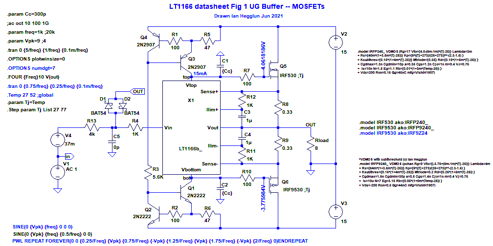
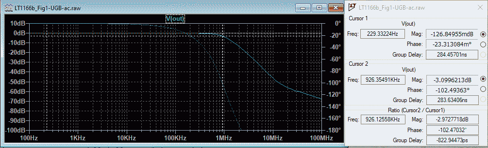
When the LT1166 is driven at the Vin pin (as below) like in the datasheet then the f-3dB is dramatically improved to about 1MHz. That's more like what we need.
The simulation files are attached.
Included is a symmetrical VAS drive which is no different BW to the Bottom VAS drive.
Also a simulation with 1uF capacitors across the Top and Bottom pins to show they kill the Auto Bias IC altogether.
A paper on my simulation of the LT1166 is here: LT1166-Bias-Controller-Follower-Simulation.pdf - Google Drive
and the LTspice files are here: LT1166-Bias-Controller-Follower-Simulation-files.zip - Google Drive
More from Syn08's post about implementing an Auto Bias loop using the LT1166 IC from here:
...one reason why ICs like the LT1166 fail short for the full audio band applications; they simply don't have enough bandwidth to keep the above rule at audio HF (if memory serves from about 10 years ago, the LT1166 is effective only to about 4KHz...
A simulations shows the LT1166 driven by a current source to the Bottom pin like a VAS would drive it.
The ac plot shows the f-3dB below as 8kHz
.
This is abysmal, pretty much unusable in this way as a drop-in Auto Bias generator. This may have been the way Syn08 used it? BTW The datasheet never showed it used in this way.
When the LT1166 is driven at the Vin pin (as below) like in the datasheet then the f-3dB is dramatically improved to about 1MHz. That's more like what we need.
The simulation files are attached.
Included is a symmetrical VAS drive which is no different BW to the Bottom VAS drive.
Also a simulation with 1uF capacitors across the Top and Bottom pins to show they kill the Auto Bias IC altogether.
A paper on my simulation of the LT1166 is here: LT1166-Bias-Controller-Follower-Simulation.pdf - Google Drive
and the LTspice files are here: LT1166-Bias-Controller-Follower-Simulation-files.zip - Google Drive
Attachments


This is abysmal, pretty much unusable in this way as a drop-in Auto Bias generator. This may have been the way Syn08 used it? BTW The datasheet never showed it used in this way.
Yes, back in 2007 😀.
https://www.diyaudio.com/forums/solid-state/94204-contribution.html#post1107005
The data sheet shows this mode in Fig. 7 and 19. That's because the distortion performance when using the VIN pin is a dismal. I can confirm (by measurements) this disappointing performance over the VIN pin, so the conclusion is the LT1166 is a no win solution 🙁.
Auto bias for class b/ab, just too complicated. It just not fun to diy.
A Vbe multiplayer with reasonable size emitter resistors at power transistors’ emitter is good enough.
I know it is compromised for simplicity.
A Vbe multiplayer with reasonable size emitter resistors at power transistors’ emitter is good enough.
I know it is compromised for simplicity.
LT1166 Vin pin
Hi Syn08,
Originally Posted by IanHegglun Post 2, "This is abysmal, pretty much unusable in this way as a drop-in Auto Bias generator. This may have been the way Syn08 used it? BTW The datasheet never showed it used in this way."
Reply by Syn08
Thanks for the link to your earlier posts. I was aware of driving the Top and Bottom pins (DS Fig 19) using an opamp, like your circuit.
But my circuit was driving the Bottom pin using a current source without any global feedback. When you use global feedback the opamps high gain takes over giving low distortion (like DC Fig 19) and wide bandwidth.
But then, how much is the LT1166 actually doing at HF if it starts to roll off at 15kHz?
The question about driving the Vin pin rather than the Top/Bottom pins -- which is it worse?
To try and answer this I used the circuit below to look at the open loop gain and phase plots. Things change with the input resistor Rin so I did several runs at 100 ohms, 1k, 5k and 100k. Notice the sources are grounded and the power rails are floating to make it open loop. The inductor is needed to maintain the same DC operating point as Rin changes.


.
With Rin 1k the open loop voltage gain is 47dB and f-3dB 15kHz. With 100 ohms it is 52dB (x400) and 15kHz. With 5k it is 37dB and 100k 12dB (all same freq). With 100 ohms the gm is 400/8=50 A/V and with 100k it is 0.5A/V. The open loop gm drops by half when Rin is about 1k.
This shows the behaviour of the Vin pin depends on what source resistance is used to drive it. If you use a current source to drive it you won't get much performance from the LT1166. If you connect it to a conventional VAS stage which is a very high resistance (at least at LF) then you need a buffer stage to get the best LF end performance with the LT1166 when driving the Vin pin.
What is the gain when driving the Top/Bottom pins?
Post 2 simulation shows you need to inject about 0.5mA into one of these nodes to get about 1A change at the output -- current gain (equiv. Hfe) of about 2000 times. BW 15kHz.
For this post the input current for 1A out is about 5mV (from1/gm= 1/200 with 1k Rin) into 1k is 5uA. That is 100th the current when driving the Top/Bottom pins in open loop. Same BW.
Why then can you get lower distortion by driving the Top/Bottom pins (as shown for DS Fig 19) and as others have proven? I think it is because driving Top/Bottom pins with an opamp and then the global feedback can bypass the LT1166 above open loop 15kHz rolloff.
Hi Syn08,
Originally Posted by IanHegglun Post 2, "This is abysmal, pretty much unusable in this way as a drop-in Auto Bias generator. This may have been the way Syn08 used it? BTW The datasheet never showed it used in this way."
Reply by Syn08
Yes, back in 2007😀
My small contribution
The data sheet shows this mode in Fig. 7 and 19. That's because the distortion performance when using the VIN pin is a dismal. I can confirm (by measurements) this disappointing performance over the VIN pin, so the conclusion is the LT1166 is a no win solution🙁
Thanks for the link to your earlier posts. I was aware of driving the Top and Bottom pins (DS Fig 19) using an opamp, like your circuit.
But my circuit was driving the Bottom pin using a current source without any global feedback. When you use global feedback the opamps high gain takes over giving low distortion (like DC Fig 19) and wide bandwidth.
But then, how much is the LT1166 actually doing at HF if it starts to roll off at 15kHz?
The question about driving the Vin pin rather than the Top/Bottom pins -- which is it worse?
To try and answer this I used the circuit below to look at the open loop gain and phase plots. Things change with the input resistor Rin so I did several runs at 100 ohms, 1k, 5k and 100k. Notice the sources are grounded and the power rails are floating to make it open loop. The inductor is needed to maintain the same DC operating point as Rin changes.
.
With Rin 1k the open loop voltage gain is 47dB and f-3dB 15kHz. With 100 ohms it is 52dB (x400) and 15kHz. With 5k it is 37dB and 100k 12dB (all same freq). With 100 ohms the gm is 400/8=50 A/V and with 100k it is 0.5A/V. The open loop gm drops by half when Rin is about 1k.
This shows the behaviour of the Vin pin depends on what source resistance is used to drive it. If you use a current source to drive it you won't get much performance from the LT1166. If you connect it to a conventional VAS stage which is a very high resistance (at least at LF) then you need a buffer stage to get the best LF end performance with the LT1166 when driving the Vin pin.
What is the gain when driving the Top/Bottom pins?
Post 2 simulation shows you need to inject about 0.5mA into one of these nodes to get about 1A change at the output -- current gain (equiv. Hfe) of about 2000 times. BW 15kHz.
For this post the input current for 1A out is about 5mV (from1/gm= 1/200 with 1k Rin) into 1k is 5uA. That is 100th the current when driving the Top/Bottom pins in open loop. Same BW.
Why then can you get lower distortion by driving the Top/Bottom pins (as shown for DS Fig 19) and as others have proven? I think it is because driving Top/Bottom pins with an opamp and then the global feedback can bypass the LT1166 above open loop 15kHz rolloff.
Attachments


Last edited:
LT1166 opamp Top/Bottom pin drive *and* Vin pin drive
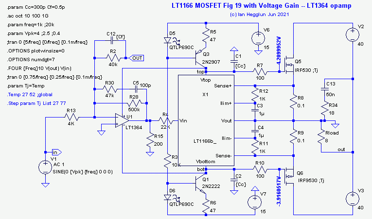
Here's a simulation of the LT1166 with an opamp driving the Top/Bottom pins and the Vin pin. Notice it uses floating PS rails so a standard voltage audio opamp can be used.
.

.
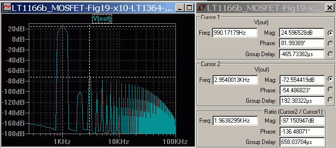
With a voltage gain of 20dB the BW is 3MHz. THD is quite low 0.002% at 1kHz.
.

.
Driving the Vin pin as well as the Top/Bottom pins adds some extra loop gain below 15kHz. R4 needs to be above 10k to prevent the LT1166 getting too confused😕. To see the effect of R4 in an ac plot replace R2 with a 1GH inductor.
Sim files are attached (including the ones for the previous post for open loop).
Here's a simulation of the LT1166 with an opamp driving the Top/Bottom pins and the Vin pin. Notice it uses floating PS rails so a standard voltage audio opamp can be used.
.
.
With a voltage gain of 20dB the BW is 3MHz. THD is quite low 0.002% at 1kHz.
.
.
Driving the Vin pin as well as the Top/Bottom pins adds some extra loop gain below 15kHz. R4 needs to be above 10k to prevent the LT1166 getting too confused😕. To see the effect of R4 in an ac plot replace R2 with a 1GH inductor.
Sim files are attached (including the ones for the previous post for open loop).
Attachments
-
 LT1166b_MOSFET-Fig19-x10-LT1364-cct.png13.2 KB · Views: 4,021
 -
 LT1166b_MOSFET-Fig19-x10-LT1364-ac.png11.4 KB · Views: 3,842
 -
 LT1166b_MOSFET-Fig19-x10-LT1364-25V-1kHz.png7.9 KB · Views: 3,880
 -
 LT1166b_MOSFET-Fig19-x10-LT1364-FFT.png10.1 KB · Views: 3,884
 -
LT1166b_MOSFET-Fig19-x10-LT1364.zip12.4 KB · Views: 182
-
LT1166b_Fig1-OL-ac.zip6.7 KB · Views: 183
Test report:
The emitter-resistor-free BJT output stage is running fine with the new temperature compensation bias circuit.
It does have a wider crossover than with the resistors, and the transistors switch later and softer, but... they do switch and they still make crossover spikes. So the quest for non-switching is still on.
Power amp OUTPUT STAGE measurements shootout
syn08 I think I've found out why you got AutoBias2 to latch up. I got it to latch up in the simulator.

If, due to some unfortunate circumstances, both Q5 and Q6 turn off at the same time... then Q1 and Q2 are only controlled by the diode transistors Q3 Q4 which means they sink a collector current of about 4mA. Since I1 and I3 source more than 4mA, Q1 and Q2 can't keep the bias voltage under control, and it rises. Since that increases the voltage across the emitter resistors, that keeps Q5 and Q6 off, which means it is latched up at the maximum bias current the power supply will provide.
If, due to some unfortunate circumstances, both Q5 and Q6 turn off at the same time... then Q1 and Q2 are only controlled by the diode transistors Q3 Q4 which means they sink a collector current of about 4mA. Since I1 and I3 source more than 4mA, Q1 and Q2 can't keep the bias voltage under control, and it rises. Since that increases the voltage across the emitter resistors, that keeps Q5 and Q6 off, which means it is latched up at the maximum bias current the power supply will provide.
Slew rate workout
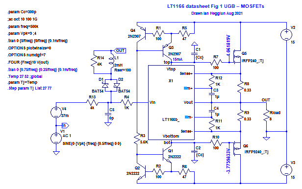
.
Without the inductor in series with the diodes the slew rate is 4V/us which limits full swing to 100kHz (below) with a sinewave (slew limiting makes it triangular)

.
With the inductor the slew rate peaks at 20V/us allowing full swing of 8Vpk at 300kHz (below)
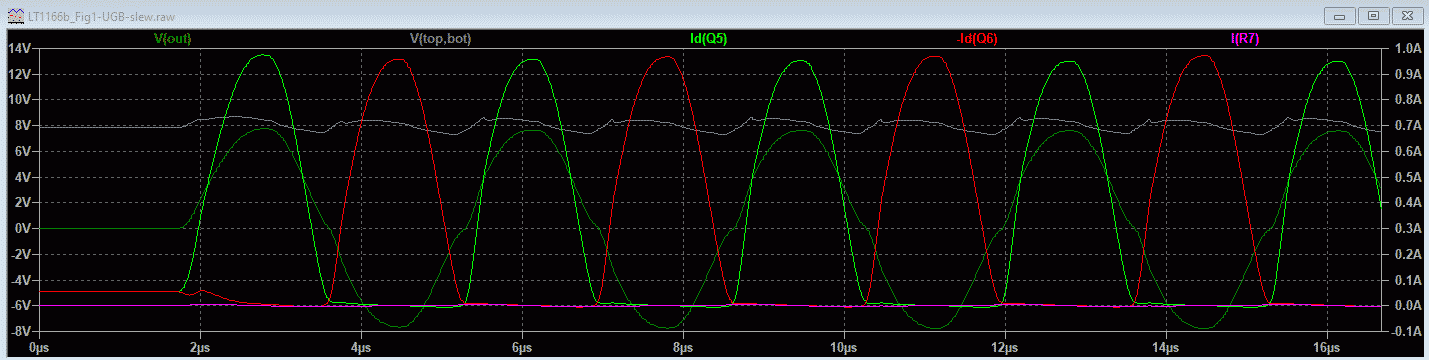
.
Now with the inductor at 500kHz the LT1166 cannot maintain its proper control and the bias voltage falls causing severe crossover distortion
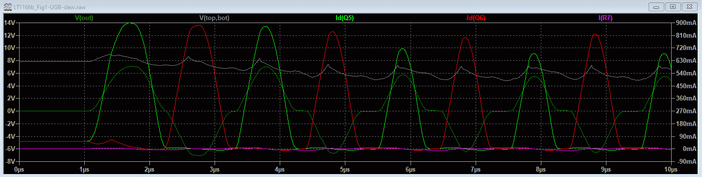
.
Notice the LT1166 when operated beyond its control limit does not give cross-conduction which is a very desirable thing for any bias system. Cross-conduction at high frequency causes excessive dissipation and usually eventual destruction as the heatsink heats up. So auto bias circuits need to be checked for cross-conduction when pushed to their limits. And driven by 1MHz the MOSFETs stop conducting after a few cycles. Looking good🙂.
This partly answers my question, that the LT1166 Vin pin drive does allow safe control of the MOSFETs even when pushed into slew rate limiting.
With higher voltage rails, like used in most power amps, the slew rate is high enough for operation to 100kHz (eg +/-50V rails), and that is without an emitter follower to drive the MOSFETs.
Looks like the LT1166 is not as bad as some have found. Looks OK for full the 20kHz.
BTW paralleling MOSFET's with a single LT1166 is not a recommended option, several IC's as "slices" should be used, like paralleling opamps, with 0.1 ohms sharing resistors to the output node.
The next question: Does that safe operation with SR limiting also apply to driving the top and bottom pins with an opamp? Yet to confirm.
I'm still thinking about this question. Some more simulations using the Vin pin. This time slew rate simulations with a 9V input - just below clip with a 15V rails using the Datasheet Fig 1 circuit again as below - but with mods to the Schottky clamp diodes for higher slew rates....my circuit was driving the Bottom pin using a current source without any global feedback. When you use global feedback the opamps high gain takes over giving low distortion (like DC Fig 19) and wide bandwidth.
But then, how much is the LT1166 actually doing at HF if it starts to roll off at 15kHz?
.
Without the inductor in series with the diodes the slew rate is 4V/us which limits full swing to 100kHz (below) with a sinewave (slew limiting makes it triangular)
.
With the inductor the slew rate peaks at 20V/us allowing full swing of 8Vpk at 300kHz (below)
.
Now with the inductor at 500kHz the LT1166 cannot maintain its proper control and the bias voltage falls causing severe crossover distortion
.
Notice the LT1166 when operated beyond its control limit does not give cross-conduction which is a very desirable thing for any bias system. Cross-conduction at high frequency causes excessive dissipation and usually eventual destruction as the heatsink heats up. So auto bias circuits need to be checked for cross-conduction when pushed to their limits. And driven by 1MHz the MOSFETs stop conducting after a few cycles. Looking good🙂.
This partly answers my question, that the LT1166 Vin pin drive does allow safe control of the MOSFETs even when pushed into slew rate limiting.
With higher voltage rails, like used in most power amps, the slew rate is high enough for operation to 100kHz (eg +/-50V rails), and that is without an emitter follower to drive the MOSFETs.
Looks like the LT1166 is not as bad as some have found. Looks OK for full the 20kHz.
BTW paralleling MOSFET's with a single LT1166 is not a recommended option, several IC's as "slices" should be used, like paralleling opamps, with 0.1 ohms sharing resistors to the output node.
The next question: Does that safe operation with SR limiting also apply to driving the top and bottom pins with an opamp? Yet to confirm.
Attachments


Why use a non-switching controller with MOSFETs when MOSFETs don't make turn-off spikes like BJTs do?
A wideband non switching Auto Bias amplifier circuit that works, doesn't oscillate and blow up, and is not too complex.
To start this thread I'll post some of my findings from simulations of the LT1166 Auto Bias IC, as well as Class-i and Edmond's AutoBias2.
Feel free to post any of your ideas and simulations.
And if anyone has built a successful amplifier using an auto bias circuit then we'd love to hear how you did it, etc.
I don't know if it meets your requirements, but my amplifier from the mid-1990's still hasn't exploded.
https://worldradiohistory.com/hd2/I...tronics-World-1996-02-S-OCR-OCR-Page-0054.pdf
https://worldradiohistory.com/hd2/I...tronics-World-1996-02-S-OCR-OCR-Page-0055.pdf
https://worldradiohistory.com/hd2/I...tronics-World-1996-02-S-OCR-OCR-Page-0056.pdf
https://worldradiohistory.com/hd2/I...tronics-World-1996-02-S-OCR-OCR-Page-0057.pdf
latch up?
Cheers, E.
Just the opposite. In that case the bias current is almost zero and if one of them (Q5 or Q6) is turned off, the bias current is about halved,syn08 I think I've found out why you got AutoBias2 to latch up. I got it to latch up in the simulator.
View attachment 971342
If, due to some unfortunate circumstances, both Q5 and Q6 turn off at the same time... then Q1 and Q2 are only controlled by the diode transistors Q3 Q4 which means they sink a collector current of about 4mA. Since I1 and I3 source more than 4mA, Q1 and Q2 can't keep the bias voltage under control, and it rises. Since that increases the voltage across the emitter resistors, that keeps Q5 and Q6 off, which means it is latched up at the maximum bias current the power supply will provide.
Cheers, E.


You have overlooked that Q1 and Q2 have a value of 2 (i.e. 2 pieces in parallel), see attachment.According to the simulator, it seems like a stable latched-up state. Where is the mistake?
Cheers, E.
Attachments

Nice, that solves the issue.
Is there a reference implementation somewhere? I would like to build one to compare to resistor-free BJTs, but I would rather not spend too much time on stability issues.
Is there a reference implementation somewhere? I would like to build one to compare to resistor-free BJTs, but I would rather not spend too much time on stability issues.
Nice, that solves the issue.
Is there a reference implementation somewhere? I would like to build one to compare to resistor-free BJTs, but I would rather not spend too much time on stability issues.
Do you see any improvement in simulation?
Hi peufeu,Why use a non-switching controller with MOSFETs when MOSFETs don't make turn-off spikes like BJTs do?
MOSFETs still have wide variations in the wingspread curves with junction temperature changes due to music power variations. Also startup of amp.
Further, a bias controller removes the necessity for the bias trimpot. With a pot there is a range of different listening outcomes for the same amp depending on were you set your pot compared to where someone sels their pot.
And one more. Variations in the MOSFET's p/n (mis)match don't matter much. The controller loop feedback removes most of these at the lower frequencies (like the 1-3kHz region). In fact, even with power BJT's controllers give almost the same wingspread plot (singular), which becomes a generic curve (it hardly changes once you pick the source resistor value). So BJT's and MOSFET's merge in their 'sound' -- and then with enough feedback the crossover distortion becomes inaudible over the whole audio range.
Well, that's ideally. But in reality lots of problems lurk with controller loops, like clip recovery and possibly unresolved stability (compensation) issues, eg, with certain types of loads and speaker cables. These problems lurk with standard amps as well but bias controllers add another layer of difficulty for these problems.
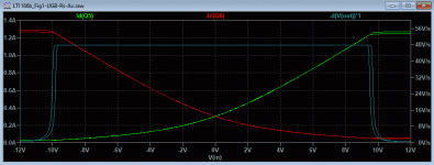
A post to follow this: showing the effect of 0.33 ohm and 0.05 ohm source resistors on the wingspread curve for the LT1166.
Effect of source resistor value on LT1166 THD
I use the circuit below
.

.
With source resistors of 0.33 ohms (as per DS Fig 1) the idle current is 55mA.
With source resistors of 0.05 ohms the idle current is 300mA.
The minimum current is trimmed by adding some offset voltage to the Sense inputs. With 50k and 10 ohms from the 15V rail the minimum current is reduced from 150mA to 50mA (thats for Rs=50mR).
The current plot for 0.33 ohms below for Tj of 27C and 77C (MOSFETs only)
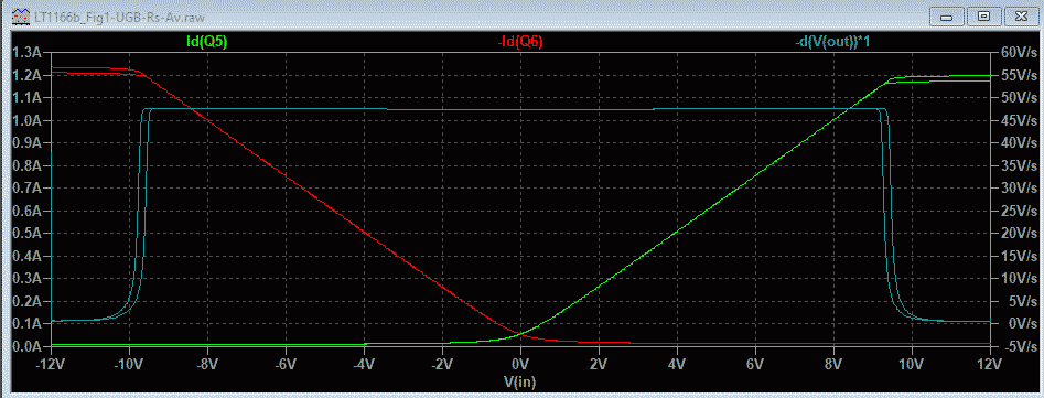
The wingspread plot for 0.33 ohms below for Tj of 27C and 77C (MOSFETs only)
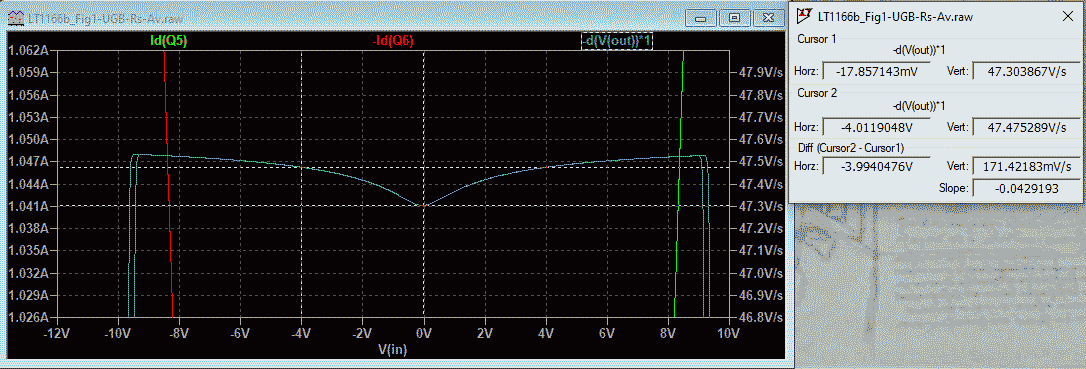
The current plot for 0.05 ohms below

The wingspread plot for 0.05 ohms below

.
Distortion figures for 0.33 ohms at 1kHz/8R are:
TJ=27 degC ..... 0.0403% and 0.0366% at 9Vpk and 4Vpk respectively
TJ=77 degC ..... 0.0408% and 0.0379% at 9Vpk and 4Vpk
Distortion figures for 0.05 ohms at 1kHz/8R are:
TJ=27 degC ..... 0.0101% and 0.0011% at 9Vpk and 4Vpk respectively
TJ=77 degC ..... 0.0095% and 0.00099% at 9Vpk and 4Vpk.
Notice how small the difference in THD is when Tj of the MOSFETs change by 50 degrees C. It is miniscule, so no thermal lag distortion and no warmup time required. That makes bias loops look so useful.
Notice with 0.05 ohm source resistors the THD for 4V peak (about 1W/8R) is only 0.001% at 1kHz. With 0.33 ohm source resistors its 30 times higher. The idle current is about 5 times higher. Looks like a worthwhile trade to me.
I use the circuit below
.
.
With source resistors of 0.33 ohms (as per DS Fig 1) the idle current is 55mA.
With source resistors of 0.05 ohms the idle current is 300mA.
The minimum current is trimmed by adding some offset voltage to the Sense inputs. With 50k and 10 ohms from the 15V rail the minimum current is reduced from 150mA to 50mA (thats for Rs=50mR).
The current plot for 0.33 ohms below for Tj of 27C and 77C (MOSFETs only)
The wingspread plot for 0.33 ohms below for Tj of 27C and 77C (MOSFETs only)
The current plot for 0.05 ohms below
The wingspread plot for 0.05 ohms below
.
Distortion figures for 0.33 ohms at 1kHz/8R are:
TJ=27 degC ..... 0.0403% and 0.0366% at 9Vpk and 4Vpk respectively
TJ=77 degC ..... 0.0408% and 0.0379% at 9Vpk and 4Vpk
Distortion figures for 0.05 ohms at 1kHz/8R are:
TJ=27 degC ..... 0.0101% and 0.0011% at 9Vpk and 4Vpk respectively
TJ=77 degC ..... 0.0095% and 0.00099% at 9Vpk and 4Vpk.
Notice how small the difference in THD is when Tj of the MOSFETs change by 50 degrees C. It is miniscule, so no thermal lag distortion and no warmup time required. That makes bias loops look so useful.
Notice with 0.05 ohm source resistors the THD for 4V peak (about 1W/8R) is only 0.001% at 1kHz. With 0.33 ohm source resistors its 30 times higher. The idle current is about 5 times higher. Looks like a worthwhile trade to me.
Attachments
-
 LT1166b_Fig1-UGB-Rs-cct.png18.3 KB · Views: 2,826
 -
 LT1166b_Fig1-UGB-Rs-330m.png10.4 KB · Views: 2,699
 -
 LT1166b_Fig1-UGB-Rs-330m-gm.png23.8 KB · Views: 2,677
 -
LT1166b_Fig1-UGB-Rs.zip9.7 KB · Views: 163
-
 LT1166b_Fig1-UGB-Rs-50m-gm.png21.8 KB · Views: 2,569
 -
 LT1166b_Fig1-UGB-Rs-50m.png8.9 KB · Views: 2,653
Hi Marcel,I don't know if it meets your requirements, but my amplifier from the mid-1990's still hasn't exploded.
Yes, it is a fantastic example of a bias loop that doesn't blow up. Thanks.
It shows your design abilities are way beyond most of ours here, including mine.
BTW did you try the LT1166, or any other discrete types? We'd love to hear any problems or success(s).
I find it interesting that about 5 of the 80 or so amplifier articles in Electronics World + WW that I surveyed (from the late 1970's to late 1990's) were not the standard topology (some call the Blameless topology, Bob Cordell calls the Thompson topology, and I call the Lin topology).
Yours is one of the five. Other 4: Ivor Brown's (Dec 1994), the Macura Follower, my Square-law Sep 1995, and Class-T. (Apologies if I missed some ones).
I'd give yours the top prize of all power amp designs in EW/WW - no kidding.
Possible amp using the LT1166
This is a follow up on the slew rate post. I have added a LTC6090 high voltage opamp as a driver for the LT1166 Vin pin (below). BTW the datasheet does not show a circuit using a high voltage opamp (closest is Fig 19 with "suspended supply operation" with lower voltage opamps that need 0.1% resistors).
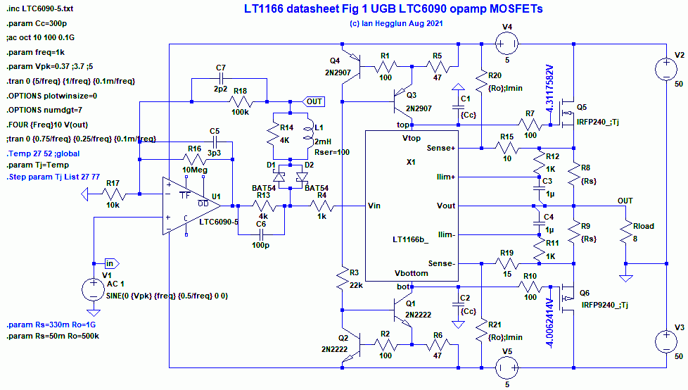
The rails are +/-50V with 5V lift for the CCS and opamp headroom, giving 40Vpk output into 4 ohms. It is 100W intended for 8 ohms.
With the LTC6090-5 the slew rate is 17V/us. This amplifier achieves 10V/us which gives full 40V at 50kHz without slew rate limiting. No cross-conduction issues at any frequency. Clip recovery OK. (BTW if the opamp was twice as fast the LT1166 should do 100kHz before slew rate limiting).
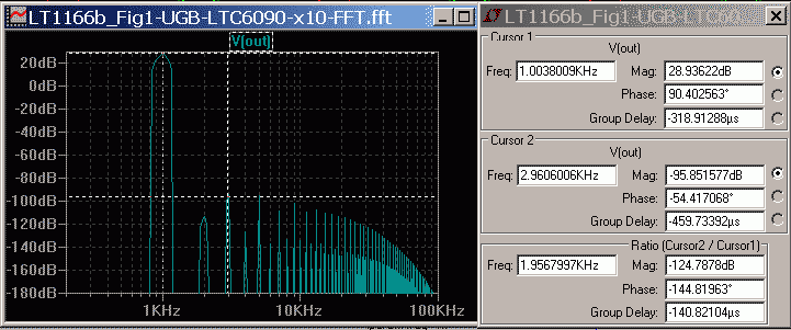
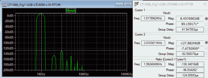
Distortion with 0.33 ohm source resistors at 1kHz: 0.00042% 40Vpk and 0.00049% 4Vpk
Distortion with 0.05 ohm source resistors at 1kHz: 0.00010% 40Vpk (FFT below) and 0.000015% 4Vpk (FFT below)
Distortion is about 10 times higher at 10kHz, and 100 times higher at 50kHz.
This is a follow up on the slew rate post. I have added a LTC6090 high voltage opamp as a driver for the LT1166 Vin pin (below). BTW the datasheet does not show a circuit using a high voltage opamp (closest is Fig 19 with "suspended supply operation" with lower voltage opamps that need 0.1% resistors).
The rails are +/-50V with 5V lift for the CCS and opamp headroom, giving 40Vpk output into 4 ohms. It is 100W intended for 8 ohms.
With the LTC6090-5 the slew rate is 17V/us. This amplifier achieves 10V/us which gives full 40V at 50kHz without slew rate limiting. No cross-conduction issues at any frequency. Clip recovery OK. (BTW if the opamp was twice as fast the LT1166 should do 100kHz before slew rate limiting).
Distortion with 0.33 ohm source resistors at 1kHz: 0.00042% 40Vpk and 0.00049% 4Vpk
Distortion with 0.05 ohm source resistors at 1kHz: 0.00010% 40Vpk (FFT below) and 0.000015% 4Vpk (FFT below)
Distortion is about 10 times higher at 10kHz, and 100 times higher at 50kHz.
Attachments


- Home
- Amplifiers
- Solid State
- Towards a wideband non switching Auto Bias power amp