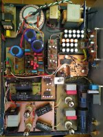
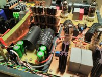
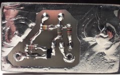
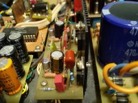
I can see that the DIY DACs has come to life, but I don't see any progress around the output-analog stage. Always the same story with passive conversion or op.amps. In contrast, here is a slightly different solution, the input lamp receives the signal at the cathode and amplifies it and sends it further to the white cathode follower which gives an output with very low resistance .Russian 6S4P with cathode resistor correction can be used instead of 6HM5. Circuit has been tested for now with the current dac PCM1702 which outputs +/- 1.2mA (similar to AD1862) , it will soon be tested with +/- 3.2mA, in fact three PCM1702 in parallel. The power supply for the tubes was performed with a serial low-noise regulator for 260V, the circuit was modified with better reference and taken from ARC LS25MKII. All other important regulators in the DAC itself are shunt type from Mr. Walt Jung with low-noise op.amps and low-noise references. Special attention in the DAC is paid to power supplies and regulators which is really heard in the final sound.
I am now working on a new DAC with a TDA1547 that will also have tubes in the output stage section.
I am now working on a new DAC with a TDA1547 that will also have tubes in the output stage section.
Attachments
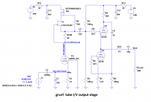
I agree that dac still sees only passive load, but there is a huge difference in the sound between the classics when we bring the signal to the grid or the cathode, ie the grounded grid. For years I believed that a classic resistor as an I / V was a good solution until I connected the 6S4P to a grounded grid. The sound became much more fluttery, more dynamic, more precise, a completely new sound image opened up. Now I use 6HM5 because it has a slightly better sound but it has some drawbacks.
As for R1, it must be as small as possible, and in this case 22R was chosen, because I will soon have three PCM1702, so this is more like a test. A higher value of R1 also results in a higher output voltage which for this tube should not exceed 10Vpp, with one PCM1702 I had 50R and an output voltage around 6Vpp and three would have a voltage around 18Vpp which would be too much. I'm even thinking of bringing 0.6V to the grid for bias and thus eliminating the influence of R1 so that it could be even smaller, then the output voltage could be around 6Vpp with a current of 7.2mApp.
As for R1, it must be as small as possible, and in this case 22R was chosen, because I will soon have three PCM1702, so this is more like a test. A higher value of R1 also results in a higher output voltage which for this tube should not exceed 10Vpp, with one PCM1702 I had 50R and an output voltage around 6Vpp and three would have a voltage around 18Vpp which would be too much. I'm even thinking of bringing 0.6V to the grid for bias and thus eliminating the influence of R1 so that it could be even smaller, then the output voltage could be around 6Vpp with a current of 7.2mApp.
Attachments
Last edited:
You can try somehing like this too:
https://www.diyaudio.com/community/...er-to-electrostatic-headphones-output.350325/
https://www.diyaudio.com/community/...er-to-electrostatic-headphones-output.350325/
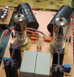
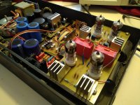
I succeeded, 6 pieces of PCM1702 are finally playing!
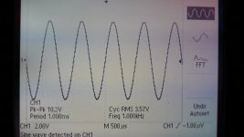
Now there are three per channel, the current is 7.2mA and the output voltage is 10Vpp, exactly as I calculated. So far I do not notice the nonlinearity of 6HM5 at such a high output voltage for this tube. The only thing I had to modify is the negative regulator, namely walt jung shunt reg according to the original scheme is designed for max current of 100mA, 6 pieces of PCM1702 now at -5V need 250mA so I replaced DN2540 with IXTP08N100 and raised the current through shunt to 350mA.
The sound is great, full of detail, open, pleasant highs without digital overtones, really pleasant sound that I doubt any DAC i.c. new generations can parry.
Attachments
Today I inserted a fixed bias for 6HM5, the negative voltage source is a 3V battery in series with CCS and a pair of diodes, the voltage can be adjusted from 0 to -1.2V. I can now set Ua and Ia separately. Now it's time to listen and then tune in a bit ")
Attachments
hi Grunf. the topology in the sch turning the phase by 180deg.
Classic Riv then tube gain stage have 0deg phase shift. As at Riv voltage is -180deg and the same for SE tube stage.
But in the grounded grid and Riv in the catode there are no "double" phase shift of 180deg.
So the signal at the output is in the opposite phase. But You can invert the DATA lines and You will have right phase...
.
IF You use preamplifier with one stage gain than leave this -180deg phase shift because preamplifier will shift "back"...
(Measure and You will see...)
.
Maybe 5687 as buffer triode will be better because of higher Anode voltage. And less complicated power supply? Because it is too much difference in Vb of buffer stage and gain stage?
cheers
I dont know seem that 6HM5 is almost linear in very small region from 0 to -1.5V Ug. After -1.5V rapidly loosing lineariy...
But with unusaly high transconductance of 20mA/V. Somehow the "sweet spot for that tube will be within -0.75V Ug, 15mA Ia and 136V Ua
.
I thik that 1000uF C at the input is not good idea. I know that must be that huge value to avoid LF filter and to have some bass. But including other 3 pass C, this make total of 4 C in the sgnal path? Maybe this is too much...
With ECC83 and 22ohm R in katode, -1.5V battery in the grid, jos 40mV is present at the DAC Io and there are no need for any coupling C?
Thanks for the interesting topic with photos of actual practical build
Last edited:
I think using AD844 as a current mirror instead of a capacitor is a good idea.I dont know seem that 6HM5 is almost linear in very small region from 0 to -1.5V Ug. After -1.5V rapidly loosing lineariy...
But with unusaly high transconductance of 20mA/V. Somehow the "sweet spot for that tube will be within -0.75V Ug, 15mA Ia and 136V Ua
.
I thik that 1000uF C at the input is not good idea. I know that must be that huge value to avoid LF filter and to have some bass. But including other 3 pass C, this make total of 4 C in the sgnal path? Maybe this is too much...
With ECC83 and 22ohm R in katode, -1.5V battery in the grid, jos 40mV is present at the DAC Io and there are no need for any coupling C?
Thanks for the interesting topic with photos of actual practical build
It will extend the LF response directly to DC. And also, since the current output impedance of AD844 is about 3MΩ, larger value of cathode resistor can be applied at the same time.
Connected the V+ to GND, V- to Iout of the DAC, and using TZ as an output, then you will get a perfect open loop current mirror.
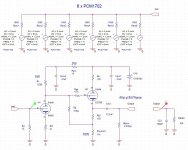
this is pretty simple output circuit for 6 x PCM1702 dac-s. With classic Riv, tube gain stage and tube buffer. Driving 10K load (or more), 4Vp-p output. Very low distortion. Phase IN output, without HF filter that could be added. One C in the path only. For 3 x PCM1702 just increase Riv to 24 ohm for the same 4Vp-p output which I consider more than enough for pream input. Or leave as 12 ohm for 2Vp-p output which is very good level for premplifier input too. (10Vp-p is just too high output level for premp input.)
cheers
cheers
Attachments
Last edited:
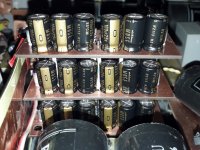
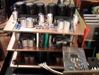
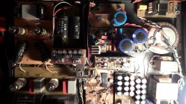
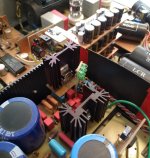
Small upgrade, the difference is in the new anode CCS, done according to Walt's article.
The CCS in the HV regulator, which supplies 14V reference, has also been upgraded.
I'm thrilled with the difference in sound, it plays great.
ax_High_Perf_Current_Regs_Revisited_0409_052921.pdf
The CCS in the HV regulator, which supplies 14V reference, has also been upgraded.
I'm thrilled with the difference in sound, it plays great.
ax_High_Perf_Current_Regs_Revisited_0409_052921.pdf
Attachments
Thanks Zoran for the advice, but I already had a similar combination with two 6S4Ps, which I switched to the grounded grid and was delighted with the difference in sound, all at Davorin's urging.this is pretty simple output circuit for 6 x PCM1702 dac-s. With classic Riv, tube gain stage and tube buffer. Driving 10K load (or more), 4Vp-p output. Very low distortion. Phase IN output, without HF filter that could be added. One C in the path only. For 3 x PCM1702 just increase Riv to 24 ohm for the same 4Vp-p output which I consider more than enough for pream input. Or leave as 12 ohm for 2Vp-p output which is very good level for premplifier input too. (10Vp-p is just too high output level for premp input.)
cheers
For now, I will stick to my schemes because I have tried a huge amount of various output stages and this is my best so far, I am not only speaking on my own behalf but on behalf of all those who have listened to it either at my place or at public presentations.
10Vp-p is OK for me because I don't use a preamplifier that I consider a redundancy component, between the DAC and the amplifier (Hiraga A class) I only have a P&G 10k log sliding pot.
Hmm, good idea, maybe I could solder something cheaper than AD844 for the test.I think using AD844 as a current mirror instead of a capacitor is a good idea.
It will extend the LF response directly to DC. And also, since the current output impedance of AD844 is about 3MΩ, larger value of cathode resistor can be applied at the same time.
Connected the V+ to GND, V- to Iout of the DAC, and using TZ as an output, then you will get a perfect open loop current mirror.
It's hard to find products with similar function. The AD844 is almost the only choice in such usage.Hmm, good idea, maybe I could solder something cheaper than AD844 for the test.
Using discrete transistor to build one in the same schematic as AD844 maybe the only alter choice. but it's difficult matching the transistors.
And by the way, I have a question.
If there's any DC bias current getting out from the Iout pin of PCM1702. And there's no outside connections for the electrons going directly to GND, which means they should find ways inside of the DAC. How much DC Voltage drift at the Iout pin would be caused?
Because I'm thinking of using a MC step up transformer as an I/V and LPF stage. If there's little DC voltage drift caused by the bias current, maybe I could connect two pieces of AD1862 in BTL, which could further reduce the voltage swing at the Iout pins.
Like this.
Hi,
For M1 what about a J310 in spite of the BSS159N
Did you try to get rid of the next tube stage bu using a voltage output controlled CCS for the anode instead a CCS ? I.e, hybrid mu follower. Story to get rid of the serie 1 uF between the 2 stages...
I wonder about the differences between the two philosophies.
There is no DC offset at the output of PCM1702, AD1862 and similar R2R dac i.c.It's hard to find products with similar function. The AD844 is almost the only choice in such usage.
Using discrete transistor to build one in the same schematic as AD844 maybe the only alter choice. but it's difficult matching the transistors.
And by the way, I have a question.
If there's any DC bias current getting out from the Iout pin of PCM1702. And there's no outside connections for the electrons going directly to GND, which means they should find ways inside of the DAC. How much DC Voltage drift at the Iout pin would be caused?
Because I'm thinking of using a MC step up transformer as an I/V and LPF stage. If there's little DC voltage drift caused by the bias current, maybe I could connect two pieces of AD1862 in BTL, which could further reduce the voltage swing at the Iout pins.
Like this.
View attachment 1044322
For the current mirror I thought of the precision N-Channel EPAD® MOSFET array, ALD series
Attachments
Last edited:
The BSS159 has a much better Vgs graph than the J309/310, almost completely flat like the BSS139 that arrived to me yesterday for new tests. BSS139 is almost the ideal candidate for the lower mosfet in the cascade thanks to a small Vgs.Hi,
For M1 what about a J310 in spite of the BSS159N
Did you try to get rid of the next tube stage bu using a voltage output controlled CCS for the anode instead a CCS ? I.e, hybrid mu follower. Story to get rid of the serie 1 uF between the 2 stages...
I wonder about the differences between the two philosophies.
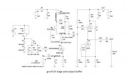
I don't bother with the number of capacitors on the signal path and my intention is to keep the WCF output stage due to its very small output impedance which is around 30ohm with ECC88.
The C2 could have been avoided by using some other tube in the output but I am very happy with the sound of the ECC88 itself so I have no intention of changing it.
Hi Grunf,
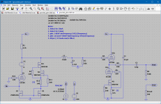
Here's a tube I-V topology I've been playing with, inspired in part by yours. Some of the features are:
I haven't built this yet, just sims, so final component selection is not complete.
Here's a tube I-V topology I've been playing with, inspired in part by yours. Some of the features are:
- Direct coupled to the CF buffer.
- The current mirror forces the AC component of the DAC output current through the grounded grid tube.
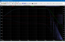
- L1, C3 and R3 are an underdamped 2nd order Butterworth filter which compensates for the sinc droop when processing 44.1k input. With this in place, HF output is extended, down -1 dB at 16kHZ.
I haven't built this yet, just sims, so final component selection is not complete.
Attachments
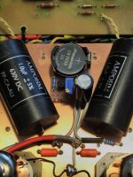
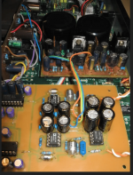
For the past two months I have been working intensively on upgrading all the regulators in my DAC. The only thing I didn't touch was the regulator of the tube heater.
The regulators for PCM1702 and PMD100 have been improved, and I didn't forget the tubes. 6HM5 and ECC88 now have much better power supplies, especially ECC88, whose regulator got a new reference instead of the 180V zener diode.
I am very satisfied with the result, especially the changes in the sound. The sound has gained a completely new dimension, incredible details and finesse that are rarely heard from digital sources. I think that the output stage without op amps is the most responsible for this, and only then the combination of PMD100+PCM1702 and excellent regulators.
Why am I writing this? Because I'm going to give the op amps another chance. But only in I/V conversion and it will be AD811 which is CFA.
My friends who regularly come to my place say that it will be difficult to beat the tubes and I say why not try. About 15 years ago I tried the AD811 and then I didn't even give it a real chance, although it was better than any VFA op.amp I tried in I/V.
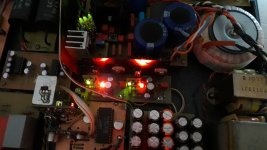
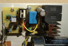
I found an old picture when I was tweaking my Rotel cd-player. In addition to the AD811, there are four more Walt superregs in the background, two for the analog part and two for the PCM1702 that replaced the PCM69.
I certainly wouldn't do it like that today, so I say that AD811 should get another chance
(Honestly, I also don't believe that it will be better than tubes but the important thing is that we have fun)
The regulators for PCM1702 and PMD100 have been improved, and I didn't forget the tubes. 6HM5 and ECC88 now have much better power supplies, especially ECC88, whose regulator got a new reference instead of the 180V zener diode.
I am very satisfied with the result, especially the changes in the sound. The sound has gained a completely new dimension, incredible details and finesse that are rarely heard from digital sources. I think that the output stage without op amps is the most responsible for this, and only then the combination of PMD100+PCM1702 and excellent regulators.
Why am I writing this? Because I'm going to give the op amps another chance. But only in I/V conversion and it will be AD811 which is CFA.
My friends who regularly come to my place say that it will be difficult to beat the tubes and I say why not try. About 15 years ago I tried the AD811 and then I didn't even give it a real chance, although it was better than any VFA op.amp I tried in I/V.
I found an old picture when I was tweaking my Rotel cd-player. In addition to the AD811, there are four more Walt superregs in the background, two for the analog part and two for the PCM1702 that replaced the PCM69.
I certainly wouldn't do it like that today, so I say that AD811 should get another chance
(Honestly, I also don't believe that it will be better than tubes but the important thing is that we have fun
)Attachments
- Home
- Source & Line
- Digital Line Level
- Tube I/V stage