You are using an out of date browser. It may not display this or other websites correctly.
You should upgrade or use an alternative browser.
You should upgrade or use an alternative browser.
My MOSFET amplifier designed for music
- Thread starter Mooly
- Start date
I was with Avantek, which at the end of my time with them became HP-AvantekI then was working at HP Signal Analysis. Some of my most valuable years.
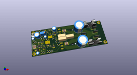
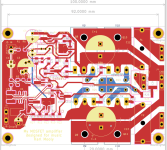
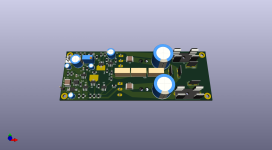
Layout with increased heat spreaders for Q3/Q5 and gate resistors now located close to MOSFET gate pads.
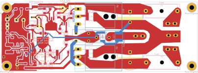
With regards to the layout at post #1615, You may have to get creative with the layout. Resistors R21 and R41 are still too far from the mosfet gate pads.
You need to get the gate resistors to within a couple of millimetres of the pads.
If you move R41 to the right of Q11 gate pad then you can move R21 to the right of Q9 gate pad where R41 is currently located.
I'm not sure if you made the pcb to a specific size but to make some room for R41 you could move the mosfets a couple of millimetres to the left.
Good suggestions. Now moved R26 slightly to make room for R41 alongside Q11 gate pad and moved R21 alongside Q9 gate pad.With regards to the layout at post #1615, You may have to get creative with the layout. Resistors R21 and R41 are still too far from the mosfet gate pads.
You need to get the gate resistors to within a couple of millimetres of the pads.
If you move R41 to the right of Q11 gate pad then you can move R21 to the right of Q9 gate pad where R41 is currently located.
I'm not sure if you made the pcb to a specific size but to make some room for R41 you could move the mosfets a couple of millimetres to the left.
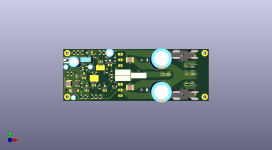
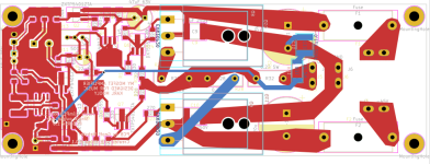
As far as the PCB overall size and location of MOSFETS/fuse-holders/connectors go, these correspond directly with Prasi's board so that this pcb could become a direct replacement for his board and fit on the side heatsink panels of a Modushop Dissipante 2U case. The prime reason for redoing the board was to future proof the Mooly design as much as possible with the ongoing removal of THT semiconductors from availability for DIY construction.
Attachments
Last edited:
I'm confused. I understood the slimmer Prasi layout, which has the same dimensions as this one, was done to suit the 2U chassis.I don't think this layout will work on a Dissipante 2U heatsink. The mounting brackets they use are 10mm to 11mm wide, so the clear space on the surface is around 58mm. This layout is 72mm. It's a better fit for the 3U chassis.
Having searched around on the Modushop site and finally found their Dissipante drawings, it looks like the clearance between the top and bottom mounting brackets is 56.3mm. As you say, this and the earlier Prasi board will fit onto the side walls of a 2U Slimline case but not onto the heatsinks of the Dissipante case.I imagine it can work in a 2U… just not the Dissipante 2U due to the mounting brackets.
If a board were laid out for a width of 50mm, it could be quite straightforward to rejig the layout for a single MOSFET pair doing this to accommodate either the single die EX10P20/EX10N20 or the double die ECW20P20/ECWN20 MOSFETs. Of interest?
I'll see what we can come up with. I'll have something to look at later tomorrow.It's something I've wanted to do. I imagine a longer skinny board similar to the layout that Rod Elliott uses on his P101 layout. Just need to find some time.
I don't think this layout will work on a Dissipante 2U heatsink. The mounting brackets they use are 10mm to 11mm wide, so the clear space on the surface is around 58mm. This layout is 72mm. It's a better fit for the 3U chassis.
I'm confused. I understood the slimmer Prasi layout, which has the same dimensions as this one, was done to suit the 2U chassis.
I hope this file can answer your questions
") "Dimensione Scasso utile interno mm" is the useful space on the heatsinks
"Dimensione Scasso utile interno mm" is the useful space on the heatsinksAttachments
Thanks Gianluca. I'd found the Dissipante drawing on your site (not an easy task) and calculated the 2U brackets had 56mm space between the top and bottom sections. 54mm useable space seems realistic as the absolute max to use.I hope this file can answer your questions
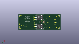
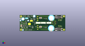
At present, I'm working on a layout for pcb outside dimensions of 100mm x 50mm. The 100mm may come down dependent on how well I squeeze components into the available space.
In line with last few posts, I've done a slim board layout (140mm x 50mm) with a single output pair. I've done the output pair footprints so that it will take either an ECX10N20/ECX10P20 pair or the double die ECW20N20/ECW20P20. The double die pair will effectively give you the same output capability as a dual output pair.
Attachments
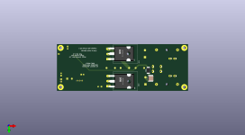
Final (hopefully) tweak of the last layout. Found enough room between the MOSFETs to site the drain resistors R27/28 closer to the MOSFET drains. Also repositioned the output resistor and Zobel network to take advantage of the space created by moving the other resistors.