Hmmmm....
AHC/AHCT Designer’s Guide September 1998
View attachment 1299529
If I read this right, the PMOS appears to have a threshold of 4.5V - 1.4V .... 5.5V - 1.6V not 0.7V.
You don't. That's the switching threshold, where the NMOS and PMOS conduct equal current.
According to the document you linked to: "The threshold voltages Vt of the transistors are, in this case, about 1 V."
Still, the typical overlap current at 3.3 V in and 5 V supply is not as bad as I thought, at least not for Schmitt trigger inputs of TI SN74AHCT chips, according to figure 6 of the same document. I guess they put a diode-connected PMOS in series with the PMOS side to reduce overlap current.
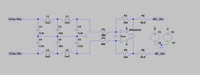
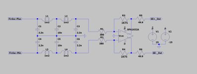
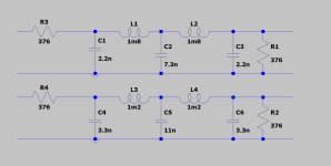
In the filter picture inductors are 1.2nH, not 1.2mH.I used a slightly larger 3.3nF input cap with 1.2mH inductors.
Here is what it ought to beIn the filter picture inductors are 1.2nH, not 1.2mH.
Hans
Attachments
In my sim it was 4.5057 ??Minor detail: the DAC reference supply is typically 4.96 V rather than 4.5 V.
Hans
Attachments
In my reality it's about 4.96 V.
I see that you are using different transistors. If their base-emitter voltage is 113.575 mV lower, that would explain the difference.
That 1.18 kohm was the value I calculated for the double transistors that were unavailable, for the BCM56DS it has to be 1 kohm.
I see that you are using different transistors. If their base-emitter voltage is 113.575 mV lower, that would explain the difference.
That 1.18 kohm was the value I calculated for the double transistors that were unavailable, for the BCM56DS it has to be 1 kohm.
Last edited:

You don't. That's the switching threshold, where the NMOS and PMOS conduct equal current.
Yes. Then I read it right. The P-Channel source connects to Vcc (say 5V). The switching voltage of the pair is at ~1.5V, where it draws maximum current.
That means the TH voltage (e.g. Id > 100uA) of the N-Channel is a little higher, say 1.7V from Vss and the TH Voltage of the P-Channel is a little lower, referenced to Vss perhaps 1.3V.
But the P-Channel transistor must reference Vcc, so it's TH voltage would need to be 3.7V.
Presumably, while 3-4V TH are common in switching Fet's, they are uncommon in logic, so perhaps a zener (connected FET) or Vgs mutiplier is implemented in the source line to shift the threshold vs a near 1V threshold.
According to the document you linked to: "The threshold voltages Vt of the transistors are, in this case, about 1 V."
Well, that statement is at odds with the observed supply current vs input voltage.
Still, the typical overlap current at 3.3 V in and 5 V supply is not as bad as I thought, at least not for Schmitt trigger inputs of TI SN74AHCT chips, according to figure 6 of the same document. I guess they put a diode-connected PMOS in series with the PMOS side to reduce overlap current.
Well, they do something. And it works.
Incidentally, the document has also data on simultaneous switching, ground bounce and many other interesting topics, that were mentioned and queried here.
Thor
R4 has to be 798R for the ZTX851 that where used in my model, that single resistor compensates for the difference.In my reality it's about 4.96 V.
I see that you are using different transistors. If their base-emitter voltage is 113.575 mV lower, that would explain the difference.
That 1.18 kohm was the value I calculated for the double transistors that were unavailable, for the BCM56DS it has to be 1 kohm.
Hans
Regarding crystal clocking of RTZ versus the XOR clock doubler, I was just getting to the point of trying that more extensively when Acko asked for the dac to be returned to him. However, my initial impression was that implementing the RTZ function with a crystal made a very obvious change to the sound. The dac started to sound much more like one of Adrea's dacs (which use crystal RTZ timing). Therefore, I wouldn't be surprised if THD would have measured differently. That said, I used clocks with SOA close in phase noise which so far as I know most people are not using.
The other thing I would say is that power supplies and USB noise have to be well taken care of or the dac ought to measure worse than it otherwise could. Unless the starting point is that all dacs to be compared are implemented identically with respect to incoming digital signal quality (cleaned of noise and stable), and implemented identically with respect to external power supply design, we will to some extent be comparing apples to oranges. IOW, we will be comparing more than just dac board differences.
The other thing I would say is that power supplies and USB noise have to be well taken care of or the dac ought to measure worse than it otherwise could. Unless the starting point is that all dacs to be compared are implemented identically with respect to incoming digital signal quality (cleaned of noise and stable), and implemented identically with respect to external power supply design, we will to some extent be comparing apples to oranges. IOW, we will be comparing more than just dac board differences.
Last edited:
A disadvantage is that when you use a crystal clock to drive the shift register, the notches of the FIRDAC are only on the right places when the bit clock frequency is half the crystal clock frequency. If you want to support a large range of DSD rates and always have notches at multiples of half the sample rate, you either need a whole bunch of crystals, or have to accept frequency dividers, or use a much longer FIRDAC.
As 1.2mH inductors are not commonly available, I would suggest this version which has slightly higher fc than my previous suggestion. Inductor can be of the same series as previously.Here is what it ought to be
Attachments
Because I used a wrong Vref on the Shift-registers, 4.5 Volt instead of 4.96 Volt, I had to redo the noise calculations and correct the gain resistor on the OPA16032 from 1K9 to 1k75 for getting 2.0V out at 0dB digital in.
Noise contribution from the OPA2210 filter is now lower because of the higher Firdac noise.
In the table S/N is shown for SE and for DM.

Hans
Noise contribution from the OPA2210 filter is now lower because of the higher Firdac noise.
In the table S/N is shown for SE and for DM.
Hans
Attachments
Yes you are right, that's why I mentioned that the 1.8mH you suggested are readily available. But because the caps in your proposal were not right for a 80Khz Butterworth, I simply took different values for the sim without looking at availability and fc.As 1.2mH inductors are not commonly available, I would suggest this version which has slightly higher fc than my previous suggestion. Inductor can be of the same series as previously.
But the inductor you proposed seems very appropriate for the job, but others may also be suited.
Hans
Attachments
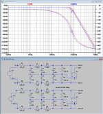
Not meant in any way to criticize you, but something seems wrong with your filter calculation program.As 1.2mH inductors are not commonly available, I would suggest this version which has slightly higher fc than my previous suggestion. Inductor can be of the same series as previously.
See the strange hickup at 80Khz versus the values that I used in Red.
Hans
Attachments
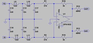
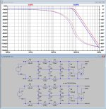
You have wrong inductor values in the lower leg.See the strange hickup at 80Khz versus the values that I used in Red.
You have wrong inductor values in the lower leg.
Sorry, I failed to correct those two inductors.
Filter Is now at 65Khz and working perfectly.
Hans
Attachments
What if I use a programmable frequency divider chip, then reclock its output using MCLK? Not all that much to it is there? I mean if DSD64, DSD128, and DSD256 are enough, I can still use pretty low close-iin phase noise clocking......have to accept frequency dividers...
Of course I need to add an MCLK input to the dac board, and maybe bring in some status signals (F0 - F3) from a USB board. Something like that.
- Home
- Source & Line
- Digital Line Level
- Return-to-zero shift register FIRDAC