Ah Ok, I wasn't sure if it was fully or part shielded, mine (from some old gear I took to bits LOL) is metal to the backpanel. They are great though, any mains LC filter like that, makes a big difference.shielded
You are using an out of date browser. It may not display this or other websites correctly.
You should upgrade or use an alternative browser.
You should upgrade or use an alternative browser.
My DIY Amplifier has a small sizzling sound
- Thread starter Sevy
- Start date
It might be mentioned that twist-rate (turns per inch) and twist tightness are two different things. Tight twists assures the wires cannot move around relative to each other. Once wires are tightly twisted they may tend to want to untwist a little. A tight tie-wrap at each end of the cable applied while the cable is twisted very tight may help to retain twist tightness over time.
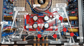
First, here are two Amplifier PCB captures; with and without the ground highlighted, the second for the silkscreen clarity. J5 is the PCB HQG connector and J2 is the speaker output connector. J1 is the input connector. J3 and J4 are +55 and -55 VDC respectively. In the casing, one PCB have it's -55 VDC in the bottom of the case and the other channel have it's -55 VDC near the top cover of the case.Do you have a picture of the internals of your amp from above with the wires labelled?
Similar for the Power Supply and Protection Circuit PCB. Notice that the speakers ground input and ground output are close together. Similarly, the speakers signal input and output are close to the relay contacts. There maybe one trace we could suspect, It's the 24 VDC trace that come close to the right speaker connectors, on the right of the PCB. I highlighted it in the third capture below, and it's the purple line in the schematic capture.
Finally, the interior of the casing as you asked, with cables identified:
Then, both Input cables are visible between the Heat-sink and the PCB on these two pictures:
In the hope that you have what you need for your observations ;-)
Hmmmh.....
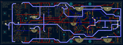
I am not an expert in pcb design and electronic, but in my opinion you have opend a door for groundloops on your pcb. The ground track in the middle of your amp pcb is not nessesary, to much crossings to other components. Left and right were enough, or only in the middle. Now the ground tracks are parallel to other ground tracks at some place. Why is the servo so far away from the input ? The tracks are rather thin. But i dont know if this is the reason for the humming effect.
I have took one picture and marked the cabling on the right side of your housing. Perhaps is possible to take a way above the input net filter to the amp pcb.
No good idea to make the cabling in this, your, way...always keep distance to the net input. Keep away from the amp input or output. Seperate all cables to each other. Secondary wires, Output wires, input wires and so on. If not possible you can cross, no parallel wiring..i think you know...
Drilling is a good idea.
The left RCA wire is very near to the secondary supply wires, perhaps touching.
If your solution with the grounding to RCA from the star point grounding has made something better, follow the advice of Bonsai or mine and solder in a filter or resistor to cinch input and the shielding.
In a bad case RCA shielding becomes active, thats the reason why XLR is the better solution. Perhaps you have got different potential on the shielding. That may the reason for humming. One reason may be the equal grounding of the input and the powersupply. This problem does not occur in every case.
Perhaps you can make a measurement of current if you split of the RCA shield and switch in a multimeter.
The second thing, easy to try, is to let one shield open at your RCA input. You have already made a connection to your star ground, if i look at the last pictures. On the first picture this connection was not done.
You can set spacers on your floorplate to get distance from net wires and secondary voltage. Its not allowed to tie the primary net wires to the metal floorplate, to dangerous...
Better with space through plastic spacers and cableties....Dont know about the canadian regulations...but thinking they are similar to the german regulations.
Because of your cabling colours i can't see if PE ist connected to your housing...for safety and EMI/EMV prevention PE should be connected.
No ideas further
Good Luck
Peter
Attachments
Last edited:
As Kleinhorn has noted: this earthing pattern is not ideal.Amplifier PCB
I would expect a line, like a single stick ladder, this seems to invite current loops.
I would consider the most sensitive parts of the amplifier are:
1. Input ground.
2. GNFB ground
Any mismatch between these two will cause hum and distortion, so in my opinion both the speaker ground and the input ground should be bonded very close to the input and feedback points, and the rest of the ampifier ground can (will) merrily flap around, as long as the associated components are aligned to it.
I.e. I'd lay out the PCB with a nice big thick tinned ground stripe in the middle, and arrange - even then - for the speaker return ground and input ground to be next to each other.
Amplifiers don't look at the signal input, they look at the difference between the signal input and ground (at each stage!). Without GNFB grounding is much easier, as only the input ground is important, but the concept should be to tie the GNFB ground and signal ground together, in my opinion, so they are always the same voltage.
Attachments
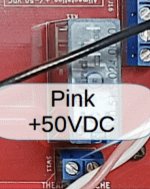
Also a note about switching 50Vdc with a single contact - what is the rating of the relay? It may be necessary to use a double pole relay and put the contacts in series, so the switching voltage then drops to 25V per contact, which it's possible to actually switch off ")
Very few relays are rated to switch off 50Vdc as they turn into arc lamps: there's a cool thread on Diyaudio about making a nice MOSFET design to do this - as most solid state relays are more expensive than simply using MOSFETS, or a triac and fuse.
For this reason I'd also put fuses between the main PSU caps and the amplifier boards, 2-3AT, so if all goes horribly wrong it's another layer of protection for the woofer coils
Attachments
Apologies for for so many comments , I have momentum... looking at the PSU schematic, my observations are:
The 2k bleeder resistors would be best replaced with current sources iMO, as they are much more efficient, and add a LED on each rail to show when active (for safety and convenience), flowing 1mA (bright enough).
ETA: Diode snubbers, best in series with 4.7R resistors, in my view.
The speaker relays as noted. The 0.22R resistors I'd also eliminate, but I'd add a small, seperate diode bridge + caps for the driver part of the power amplifier boards, so voltage sags from the main transistors do not drag down the rails of the driver section.
I would also add a soft-start relay on the 220Vac line, with a 56R 10W resistor of about 6 seconds, for a nice gentle startup.
, I have momentum... looking at the PSU schematic, my observations are:The 2k bleeder resistors would be best replaced with current sources iMO, as they are much more efficient, and add a LED on each rail to show when active (for safety and convenience), flowing 1mA (bright enough).
ETA: Diode snubbers, best in series with 4.7R resistors, in my view.
The speaker relays as noted. The 0.22R resistors I'd also eliminate, but I'd add a small, seperate diode bridge + caps for the driver part of the power amplifier boards, so voltage sags from the main transistors do not drag down the rails of the driver section.
I would also add a soft-start relay on the 220Vac line, with a 56R 10W resistor of about 6 seconds, for a nice gentle startup.
Last edited:
Input and General wiring.
Looking at your input wiring, it seems you have the signal + signal return going to the amp modules via the black-screened cables, and then you have joined the signal grounds and connected them to the star ground with the white wire. This means you have very large input circuit loop areas and two grounding points so highly likely a common impedance coupling problem as well. The signal grounds must go back to the amp modules and nowhere else.
I would not route the input cables under the base plate. Run them around the top of the amplifier above the PCB and right next to the chassis. You want to keep the loop between the signal ground, the chassis and all other 0V bounded areas as small as possible (leaving aside the loop areas on the PCB for now).
I agree with other comments that your mains wiring is too close to the amp module that appears on the RHS of the image (the left channel I think). You should try to reconfigure that.
If you have not fitted an HBR, then you should do it - see the picture below and note very carefully how it is done. It is not just a resistor in series with the signal return. If you do it like that, you will make your problems worse. To fit it, you will need to cut some tracks on your PCB. I recommend a value of 2.2 to 4.7 Ohms. The benefit comes from the voltage divider action offered by the HBR and the signal ground DC resistance. If you use a 2.2 Ohm HBR and your signal ground wiring (from source) is say 100m Ohms, you get theoretically 26 dB reduction in cross channel ground loop current generated noise voltages.
PCB Layout.
The kind of layout you have used I call a 'folded' layout (the other way is with all the output transistors in a line). The important thing is to keep the V+, output rail and 0V tracks for the positive side and then the V-, output rail and 0V tracks on the -ve side very close together. Lay the V+ and V- tracks over the output rail track and keep the 0V (which you use for decoupling) right next to these. This way, the radiating loop areas for the output and decoupling are kept small and the result is lower noise and lower distortion (The distortion arises because the high output currents generate large mag fields that couple into the small signal areas of the amp). In your layout, you show a central ground track going to the input circuit. This is the correct way to do it, with the following caveats. This signal ground track must run under the feedback and gain setting resistors - again, to keep the loop arwea as small as possible. The gain setting resistor is returned to the signal ground trace through the HBR and the input signal; ground connects to the other side (ie not the signal ground trace side) of the HBR. Again, keep the input circuit loop areas as small as possible. Do not connect any other components to this signal ground trace. If you put your decoupling capacitor returns, you will cause excess noise.
One other point is where you take the speaker return to on your PCB - locate it on the other side of the connection back to the PSU Module. if you put it on the same side as the PCB 0V return, you will create distortion through common impedance coupling.
I attached another picture at the bottom to hopefully clarify these things. I think before you look outside your amp, you have to get it absolutely silent on both channels.
PSU board
A learning point here is that on the PSU board always overlay the traces going to the reservoir caps over each other and keep the caps as close together as possible. Very large charging currents are flowing from the transformer to the reservoir capacitors and these will be generating significant mag fields that will couple into the small signal loops in your wiring and on the amp PCB. On a 100W amplifier, full-power charging currents of >10A are quite normal and full of high level harmonics up to 1 kHz.
Last edited:
Ouffff!
You guys are talking about redoing a totally new PCB! I am not ready for that lol. This PCB is my second real attempt after a bad choice on a first circuit took from a book that wasn't working at all. See the history shared in post #64. And I have done a couple of iterations before concluding with this setup. Anyway, I guess my choices need further explanations.
First, the bigger challenge was to put al three stages; IPS, VAS and OPS on a single PCB that would fit into the heat-sink area of a 3U case.
Now if I read back all your observations and comment them...
Keep in mind the HQG start setup, as showed here:

The goal was to separate all grounds to respect the above setup on the PCB.
The decision to include a DC servo as been made at the end of the design. So I tried to put it where I had space left. In my opinion, it wasn't as crucial as other sections regarding it signal and ground path. As the limiting dimensions mentioned above, the four can capacitors could not be placed close to each others for their ground to be as close as possible without sacrificing others grounds issues. My priority was always to keep the star setup before anything else.
Trust me. I tried all possible path with the headphone on my ears and the RCA loop-back connected on both inputs. The final actual path is the lest noisy.
I tried to pass the signal wire above the AC socket and it was worst.
When I play/move all the wires with my hand, I don't hear difference.
This has been already tested and it is worst if I disconnect it.
I'll do that.

The relays doesn't switch the 50 VDC! They switch in and out the Speakers. I use model FINDER-40.51 that are rate at 12 A and 250 VAC. See attached PDF.
All yours observations are additions that I'll keep in mind after all the books reading I have already done. I understand that there are a lots of solutions and that at some point every individual have to choose one particular design from all the available ones.
You guys are talking about redoing a totally new PCB! I am not ready for that lol. This PCB is my second real attempt after a bad choice on a first circuit took from a book that wasn't working at all. See the history shared in post #64. And I have done a couple of iterations before concluding with this setup. Anyway, I guess my choices need further explanations.
First, the bigger challenge was to put al three stages; IPS, VAS and OPS on a single PCB that would fit into the heat-sink area of a 3U case.
Now if I read back all your observations and comment them...
I am not an expert in pcb design and electronic, but in my opinion you have opend a door for groundloops on your pcb. The ground track in the middle of your amp pcb is not nessesary, to much crossings to other components. Left and right were enough, or only in the middle. Now the ground tracks are parallel to other ground tracks at some place.
Keep in mind the HQG start setup, as showed here:
The goal was to separate all grounds to respect the above setup on the PCB.
Why is the servo so far away from the input ? The tracks are rather thin. But i dont know if this is the reason for the humming effect.
The decision to include a DC servo as been made at the end of the design. So I tried to put it where I had space left. In my opinion, it wasn't as crucial as other sections regarding it signal and ground path. As the limiting dimensions mentioned above, the four can capacitors could not be placed close to each others for their ground to be as close as possible without sacrificing others grounds issues. My priority was always to keep the star setup before anything else.
I have took one picture and marked the cabling on the right side of your housing. Perhaps is possible to take a way above the input net filter to the amp pcb.
Trust me. I tried all possible path with the headphone on my ears and the RCA loop-back connected on both inputs. The final actual path is the lest noisy.
I tried to pass the signal wire above the AC socket and it was worst.
No good idea to make the cabling in this, your, way...always keep distance to the net input. Keep away from the amp input or output. Seperate all cables to each other. Secondary wires, Output wires, input wires and so on. If not possible you can cross, no parallel wiring..i think you know...
Drilling is a good idea.
The left RCA wire is very near to the secondary supply wires, perhaps touching.
When I play/move all the wires with my hand, I don't hear difference.
The second thing, easy to try, is to let one shield open at your RCA input.If your solution with the grounding to RCA from the star point grounding has made something better, follow the advice of Bonsai or mine and solder in a filter or resistor to cinch input and the shielding.
In a bad case RCA shielding becomes active, thats the reason why XLR is the better solution. Perhaps you have got different potential on the shielding. That may the reason for humming. One reason may be the equal grounding of the input and the powersupply. This problem does not occur in every case.
Perhaps you can make a measurement of current if you split of the RCA shield and switch in a multimeter.
The second thing, easy to try, is to let one shield open at your RCA input. You have already made a connection to your star ground, if i look at the last pictures. On the first picture this connection was not done.
This has been already tested and it is worst if I disconnect it.
You can set spacers on your floorplate to get distance from net wires and secondary voltage. Its not allowed to tie the primary net wires to the metal floorplate, to dangerous...
I'll do that.
It is...Better with space through plastic spacers and cableties....Dont know about the canadian regulations...but thinking they are similar to the german regulations.
Because of your cabling colours i can't see if PE ist connected to your housing...for safety and EMI/EMV prevention PE should be connected.
Also a note about switching 50Vdc with a single contact - what is the rating of the relay? It may be necessary to use a double pole relay and put the contacts in series, so the switching voltage then drops to 25V per contact, which it's possible to actually switch off
Very few relays are rated to switch off 50Vdc as they turn into arc lamps: there's a cool thread on Diyaudio about making a nice MOSFET design to do this - as most solid state relays are more expensive than simply using MOSFETS, or a triac and fuse.
The relays doesn't switch the 50 VDC! They switch in and out the Speakers. I use model FINDER-40.51 that are rate at 12 A and 250 VAC. See attached PDF.
For this reason I'd also put fuses between the main PSU caps and the amplifier boards, 2-3AT, so if all goes horribly wrong it's another layer of protection for the woofer coils
Again, this is a totally new design... I am not ready to go in this path...Apologies for for so many comments
The 2k bleeder resistors would be best replaced with current sources iMO, as they are much more efficient, and add a LED on each rail to show when active (for safety and convenience), flowing 1mA (bright enough).
My future design will surely include resistors in the snubbers. Although it is the first time I see resistors in series with the snubbers capacitors, but I admit it is my first Audio Power Amplifier Supply.ETA: Diode snubbers, best in series with 4.7R resistors, in my view.
Here in Canada we used 120 VAC.The speaker relays as noted. The 0.22R resistors I'd also eliminate, but I'd add a small, seperate diode bridge + caps for the driver part of the power amplifier boards, so voltage sags from the main transistors do not drag down the rails of the driver section.
I would also add a soft-start relay on the 220Vac line, with a 56R 10W resistor of about 6 seconds, for a nice gentle startup.
All yours observations are additions that I'll keep in mind after all the books reading I have already done. I understand that there are a lots of solutions and that at some point every individual have to choose one particular design from all the available ones.
Attachments
This is the blessing, and the curse of DIY: everything can always be alterednew PCB
Often this ends up with 'I'll build a MKII' and so it goes on
In a fault condition - one MOSFET welding itself shut, there may be 50V across the speaker...The relays doesn't switch the 50 VDC! They switch in and out the Speakers.
120Vac, apologies, I thpought France, from the language
For 120Vac I'd then use 27R.
All are suggestions, of course, this is a hobby and supposed to be fun, not constant work, I myself have a huge list of improvements for my stuff too, if only the days were longer! As you are designing the PCBs, you have the luxury of making quite big changes per iteration, I should probably look at doing that too, for my stuff, when funding permits!
Here is a good thread about choosing relays for speaker protection.
https://www.diyaudio.com/community/...tion-what-spec-should-i-be-looking-at.392082/
There's actually a few threads, it's a whole science in itself, and some elegant MOSFET based solutions. As I am not laying out new PCBs and already have a cheap relay based protector board, I just added 2AT fuses to the rails, but if I do get around to designing a new board I'll include two MOSFET protectors..
Input and General wiring.
Looking at your input wiring, it seems you have the signal + signal return going to the amp modules via the black-screened cables, and then you have joined the signal grounds and connected them to the star ground with the white wire. This means you have very large input circuit loop areas and two grounding points so highly likely a common impedance coupling problem as well. The signal grounds must go back to the amp modules and nowhere else.
I totally agree with you but as already mentioned, if I lift either of the ground end at the Amp module, or at the white cable star point, the noise is worst. The best result I get is with both connected but I do understand the loop it create.
I would not route the input cables under the base plate. Run them around the top of the amplifier above the PCB and right next to the chassis. You want to keep the loop area between the signal ground and the chassis as small as possible (leaving aside the loop areas on the PCB for now).
I could try that...
I agree with other comments that your mains wiring is too close to the amp module that appears on the RHS of the image (the left channel I think). You should try to reconfigure that.
Got it
That's the part I hate, cutting the pcb lol... It means I cannot think of it as finished. All those recent comments start to make me think of making a totally new design... $$$$,$$If you have not fitted an HBR, then you should do it - see the picture below and note very carefully how it is done. It is not just a resistor in series with the signal return. If you do it like that, you will make your problems worse. To fit it, you will need to cut some tracks on your PCB. I recommend a value of 2.2 to 4.7 Ohms.
PCB Layout.
The kind of layout you have used I call a 'folded' layout (the other way is with all the output transistors in a line). The important thing is to keep the V+, output rail and 0V tracks for the positive side and then the V-, output rail and 0V tracks on the -ve side very close together. Lay the V+ and V- tracks over the output rail track and keep the 0V (which you use for decoupling) right next to these. This way, the radiating loop areas for the output and decoupling are kept small and the result is lower noise and lower distortion (The distortion arises because the high output currents generate large mag fields that couple into the small signal areas of the amp). In your layout, you show a central ground track going to the input circuit. This is the correct way to do it, with the following caveats. This signal ground track must run under the feedback and gain setting resistors - again, to keep the loop arwea as small as possible. The gain setting resistor is return to the signal ground trace through the HBR and the input signal; ground connects to the other side (ie not the signal ground trace side) of the HBR. Again, keep the input circuit loop areas as small as possible. Do not connect any other components to this signal ground trace. If you put your decoupling capacitor returns, you will cause excess noise.
One other point is where you take the speaker return to on your PCB - locate it on the other side of the connection back to the PSU Module. if you put it on the same side as the PCB 0V return, you will create distortion through common impedance coupling.
I attached another picture at the bottom to hopefully clarify these things. I think before you look outside your amp, you have to get it absolutely silent on both channels.
That will be another nice project for my retirement!
Thank every ones for all the advises...
Sevy,
I agree with you but as already mentioned, if I lift either of the ground end at the Amp module, or at the white cable star point, the noise is worst. The best result I get is with both connected but I do understand the loop it create.
Then you have to consider you have some other serious problem that you need to fix. Is the signal ground connected on the amp module side? Can also be that the loop on your PCB is MUCH larger than the loop you have between the input connectors and the power wiring. I can't speak for Randy Slone (RIP) or Douglas Self's layouts, but the image below is for a 60W class A amplifier running 2.2Ams standing current per channel (total 4.4 Amps). You can see the peak mains component is at -126 dBr. This amp uses the layout techniques I showed in the presentation I linked to earlier with a big focus on keeping loop areas as small as possible. In class AB operation, the peak mains component is 2-3 dB lower.

Unfortunately, getting noise down to really low levels requires quite a learning curve - there is no other way for it but to burn your fingers a bit and then try again. Anyway, I hope you make progress!
I agree with you but as already mentioned, if I lift either of the ground end at the Amp module, or at the white cable star point, the noise is worst. The best result I get is with both connected but I do understand the loop it create.
Then you have to consider you have some other serious problem that you need to fix. Is the signal ground connected on the amp module side? Can also be that the loop on your PCB is MUCH larger than the loop you have between the input connectors and the power wiring. I can't speak for Randy Slone (RIP) or Douglas Self's layouts, but the image below is for a 60W class A amplifier running 2.2Ams standing current per channel (total 4.4 Amps). You can see the peak mains component is at -126 dBr. This amp uses the layout techniques I showed in the presentation I linked to earlier with a big focus on keeping loop areas as small as possible. In class AB operation, the peak mains component is 2-3 dB lower.
Unfortunately, getting noise down to really low levels requires quite a learning curve - there is no other way for it but to burn your fingers a bit and then try again. Anyway, I hope you make progress!
Last edited:
Hi Sevy,
i am a beginner with KiCad and pcb layout too....my problem is that i make an upload with the gerber files i am always too fast. By a second or third look i always find things to make something better. Sometimes little things, but it bothers me. I want to improve and make the next upload...
You have got many advices now and i would decide to make a new layout. But it's your thing...
I do not want to live with some hum...
Will say ..your not alone with new pcb's....
Greets
Peter
Hi Kleinhorn,
For my part, I am not new at all with PCB designs. I have done a numbers in the past. Three Tube Pre-Amp boards, one Tube RIAA board, three different Power Supply's for them, not to mention some splitters designed for a RF company in the 1982, and of course these two boards with this project.
But I admit that it's my first big project, with all the case ground loop problems.
I have the same problem as you, I am to much excited sometime to see the result and upload the gerber file to fast. Plus, I am a draftsman with more than 30 years experience with AutoCAD, with some of them with electronic schematics. So I have hard time to design a PCB without symmetry and/or esthetic patterns. And it seem apparently that for a Power Amplifier, we must put aside all theses criteria ;-)
I cut/pasted all the comments above and putted them in a spreadsheet that I will study deeper. I am already thinking to try to invert everything from front to rear of the case, transformer, Power Supply PCB, in the goal to get the Input closer to the RCA connector.
The thing that bother me is, this actual setup may look very bad but, at 65 years olds (in two months) I don't hear any difference in the sound between my DIY and my Rotel Amplifiers, excepted for the left channel tiny tiny tiny little noise, that is totally covered as soon as an audio material is playing! Even without material, I cannot hear it unless I bring my ear close to the speaker. So would I hear any more difference making all these new design changes?!
Anyway, I will retire in two months and will have plenty of time playing with KiCad to redo the PCB based on the above comments. And if I want to proceed, I will only have to send the gerber files and pay the price lol.
YesSo would I hear any more difference making all these new design changes?!
My view is that these loops also come alive when the music is playing, but to a greater degree than when the amplifier is just idling.
So the quietness is a symptom, but not the main cost: the cost will be sound quality when real currents start flowing.
That your very first big project matches a top Rotel amplifier is pretty impressive, and shows the potential of DIY!! That's a very very good result!
As for symmetry, I don't see why that should not be welcomed in a PCB, the +ve and -ve sides are in general, symmetrical in many respects
Often, as we see in the old era (mud-flood) buildings, form and function show huge beauty. The actual setup you have looks good, tidy, neat, safe. But everything can be improved, especially when many people on DIYaudio look for tiny things to be improved . In the meantime, some of the grounds on the PCBs could perhaps be solidified with added wires on the bottom, it just depends how much time you can bear re-working. I would suggest living with it for a few days first, as there may also be other changes - bass response caught me out recently - extending too low, causing issues with some vinyl vs flapping woofer cones...
I think this effect is some universal property of this universe / school / matrixi make an upload with the gerber files i am always too fast. By a second or third look i always find things to make something better.
The problem here is the space available onto the heat-sink surface. The PCB is much longer than it is high. So passing traces from left to right (front to rear of the case) is very limited by this height with all the components and others traces occupying the surface. Not to mention the mounting holes of the transistors and the PCB itself onto the heat-sink. Then one PCB rule design is to always stop and start from a part donuts, the least possible from an existing trace.As for symmetry, I don't see why that should not be welcomed in a PCB, the +ve and -ve sides are in general, symmetrical in many respects
To all of you who have said very good comments about the ground, +V and -V, I invited you to have a more deeper look at the PCB design and to concentrate yourself to the empty free space on it. You should observe how much it is crowd. Then, if you keep in mind all the rules to observe, Input connector far from the Output and rails ones, speaker ground close to Input ground and to feedback ground. +V, -V and ground close together, reaching all components...
You'll realize that in that space, it's a real puzzle, but fun!
And it's not like I didn't tried ;-)
In the picture below, I have activated the Courtyard layer in magenta. KiCad does permit you to transgress this rule: no magenta line must touch another. It is the safe part space...
Last edited:
Sevy, we have the same Age then...
Kicad is new to me, using now for a few months. I have fun, making pcb's for my own use. In my job in the past i was an electrican with master craftsman's diploma, not much to do with electronic. Now as a pensioner i can spent much time in this wonderfull hobby.
I cross my fingers that you can find a solution.
Greets
Peter
Could just mean you have other problems in your system, which are masking the differences between amplifiers. Don't give up, is all.I don't hear any difference in the sound between my DIY and my Rotel Amplifiers,...