Hi,
continuing from this thread I would like to open a new thread about interfacing a TDA1541 based DAC to a PMD100 based frontend, but the information about this topic seems to be lost. Here are the links I found:
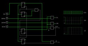
Attached screen shots of the simulations where the timing of the created LE signal is shown.
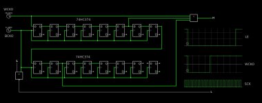
EDIT:simulation of PMD100 glue logic for stand alone mode. Post #102 gives a summary of the reclocked glue logic circuit I installed into my Arcam Delta Black Box v.1, post #228 contains the final simulation, #229 the latest mcu code to configure the PMD100 in programmed mode and the latest schematics, #230 shows the final state of my Arcam.
continuing from this thread I would like to open a new thread about interfacing a TDA1541 based DAC to a PMD100 based frontend, but the information about this topic seems to be lost. Here are the links I found:
- Nakamichi glue logic
- philpoole's information
- guido's solution
- some useful diagrams about how to interface the TDA1541A
- SM5813 to TDA1541
- SM5813 to TDA1541 follow up
- PMD100 to TDA1541A
- PMD100 to TDA1541A follow up 1
- PMD100 to TDA1541A follow up 2
Attached screen shots of the simulations where the timing of the created LE signal is shown.
EDIT:
Attachments
Last edited:
No, the datasheets for the PMD100 and TDA1541A are still out there.the information about this topic seems to be lost.
No, the datasheets for the PMD100 and TDA1541A are still out there.
Good joke
")
Joking aside, it is an interesting strategy to omit the sources of information that are guaranteed to enable you to complete the task at hand.
Here they are. But they don't tell me which logic IC is the right one for the JP-type version of the circuit: do you know the answer? If yes please direct me to the datasheet
Attachments
That is not the role of the datasheet. The PMD100 datasheet gives you the output options and the TDA1541A datasheet gives you the input options. It is for you to choose the appropriate options and make them work together. As to the JP-type version of the circuit, I haven't a clue as to what that is.But they don't tell me which logic IC is the right one for the JP-type version of the circuit: do you know the answer? If yes please direct me to the datasheet
Sorry, a typo: I meant JK. Obviously you didn't bother to read the first post, otherwise you would have noticed the version with JK-type flipflops and the question about them. And thanks for pointing out the datasheet: you seem to think we didn't know that. I recommend you PM me with your contributions unless they are of help for the topic - that would save space here and make the forum better readable for future research...
Last edited:
LE comes after last falling edge of BCK (during LSB) and before next MSB. That is what the datasheet is showing. The timing of PMD100 differs from that, and the glue logic translates between the two. You seem to indicate that one or more of the shown circuits violate timing spec: if so, why not giving clear words?
What the Philips datasheet shows is a clock and data set that meets all the stated timings including a minimum BCK cycle time of 156nS. As the data is simultaneous there is only one frame and it is 16 bits long therefore BCK is continuous at 16Fs. The PMD100, OTOH, uses the stopped clock method so there is only one clock cycle per active bit. The clock burst is always 32Fs which violates the minimum BCK cycle time but it still meets the data setup time which is probably why it still works. Point is so long as all 16 bits are loaded before the rising edge of LE the dac doesn't care.
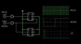
I agree. The simulation of the circuit with the JK-type flip flops in my first post shows DATA half a cycle delayed in order to get the falling edges of BCKO in the middle of the DATA pulses. I think that should be correct. The Nakamichi circuit has even better timing but uses DG to generate LE - as far as I understand the PMD100 data sheet WCKO has the lowest jitter of all output lines, hence the JK circuit uses WCKO to create LE. I wonder if I could omit the inverter and use LE to reset the middle flip flop...?
Last edited:
Yes I will try. But which version...? Looking at the simulations my findings are so far:
- the Nakamichi circuit uses DG to create LE, but the PMD100 data sheet says WCKO has the lowest jitter;
- same with the SM5813 glue logic (BTW: SM5813 seems to have the same timing as PMD100 and YM3414); plus it just inverts BCKO instead of delaying DATAL / DATAR;
- my JK-flipflop based circuit creates LE from WCKO and has the timing between DATA and SCK sorted, but LE is a bit short and I am not sure if any forbidden conditions of the logic ICs are protected correctly...
Last edited:
I built some of the circuits: one inverting WCKO and BCKO, the JK-type circuit and a D-type FF version. All of them seem to work identically: I can hear the music with very low volume and loud crackling noise from both channels.
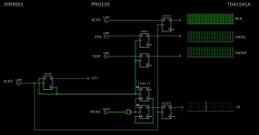
The TDA1541A is fine (tested from an SAA7220). I configured it for simultaneous mode and pulled the COB pin at the PMD100 low.
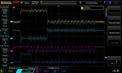
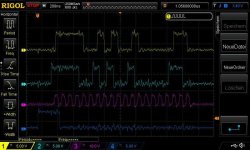
Here are some scope shots:
inverted.jpg: yellow = wcko_inv, green = wcko, red = bcko_inv, blue = LE created with JK-flipflop (DATA not shown)
reclocked.jpg: yellow = dataR_delayed, green = dataR, red = bcko, blue = LE creted with JK-flipflop
(the screen shots are taken before I configured the PMD100 for 16bit output...)
The TDA1541A is fine (tested from an SAA7220). I configured it for simultaneous mode and pulled the COB pin at the PMD100 low.
Here are some scope shots:
inverted.jpg: yellow = wcko_inv, green = wcko, red = bcko_inv, blue = LE created with JK-flipflop (DATA not shown)
reclocked.jpg: yellow = dataR_delayed, green = dataR, red = bcko, blue = LE creted with JK-flipflop
(the screen shots are taken before I configured the PMD100 for 16bit output...)
Attachments
Last edited:
- Home
- Source & Line
- Digital Line Level
- PMD100 to TDA1541 in smultaneous mode