Thanks Marcel, Always something to learn from your posts.
I like the Rega design very much, but it is quite obvious that it does not lend itself easily to be optimized with selectable input stage current.
A much more conventional input stage like the one used by NAD lend itself better to this. Specifically, The NAD LTP stage has about 300uA tail current in MM mode and about 6mA tail current thru the un-obtainium 2SB737 with MC strapping (stap-8).
Since the system has servo from output to stage #1 the 2800 ohm source resistance is achieved by DC coupling between the two stages (passive LP filter achieved by 2800R / 27nF capacitor).
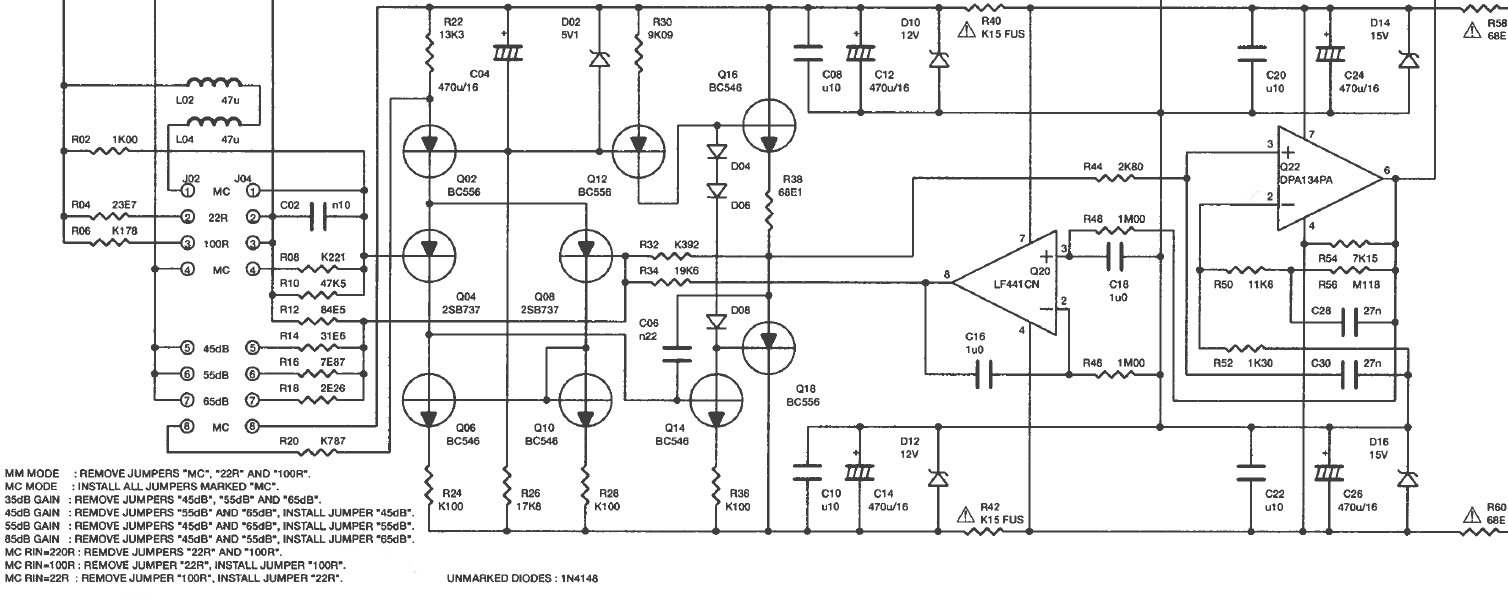
I wrote about partly decoupling R231 and R232 in post #39, but you could also completely decouple them. At least I don't see anything that would go wrong if you did, especially at low collector currents.
I have no idea how much the forward voltage of an LED changes over its lifetime. You could change the current sources in the red boxes into VBE-based sources to at least make the currents track the currents through R231 and R232 over temperature.
Regarding DC servos and RIAA correction, the feedback shifts the RIAA correction poles (not the zero, just the poles). You either have to precorrect the poles so they end up at the right places after the shift, or to ensure the DC servo has very little loop gain left at 50 Hz (like -40 dB or so if you allow a 1 % error), or to put an inverse RIAA network in the feedback path of the DC servo.
See also my extended graph here [ https://www.patreon.com/posts/90783025 ] , and read Wiki here [ https://en.wikipedia.org/wiki/Magnetic_cartridge ] :Thanks Nick for the graphs,
- MC cartridges offer very low inductance and impedance, which means that the effects of capacitance (in the cable that goes from the cartridge to the preamp) are negligible, unlike MM cartridges, which comparatively sport very high inductance and impedance. In the latter, cable capacitance can negatively affect the flatness of frequency response and linearity of phase response. This would account for a potential sonic advantage to MC types.
- It is generally believed that MC cartridges sport lower moving masses. However, quality MM cartridges are able to offer as low or lower moving mass than some MC cartridges. For example, the state-of-the-art Technics EPC-100CMK4 with 0.055 mg of effective tip mass, of moving magnet design. Comparatively, the popular Denon DL-301 moving coil cartridge has an effective tip mass of 0.270 mg.
"
Last edited:
Since field-effect transistors input for MM cartridges are definitely better than bipolar ones, it seems to me that the switching solution used in Kenwood L02 is more radical and circuitry is much more justified 🤓The NAD LTP stage has about 300uA tail current in MM mode and about 6mA tail current thru the un-obtainium 2SB737 with MC strapping
Attachments
Nick, that's a good input stage and shows the importance of masking and listening tests between BJT masking and JFET masking, the idea is that the signal coming through should be higher that the noise in the pickup process. This gives LPs that aura in the playback process. Although the BJTs should be in odd numbers say 3,5,7 etc This is what I had suggested Joe try
Masking is resolution control technique that acts as a filter.Thank you OnAudio for your reply.
What do you mean by "masking"? The high input isolation offered by the cascode gain stage or ?
You saved me a lot of time there as I was going to do some binning on these! However I guess there is still a need to match the complementary pairs in Hfe?
Just throw them in there. May I suggest you try five. The control board can be matched. Then AB test them
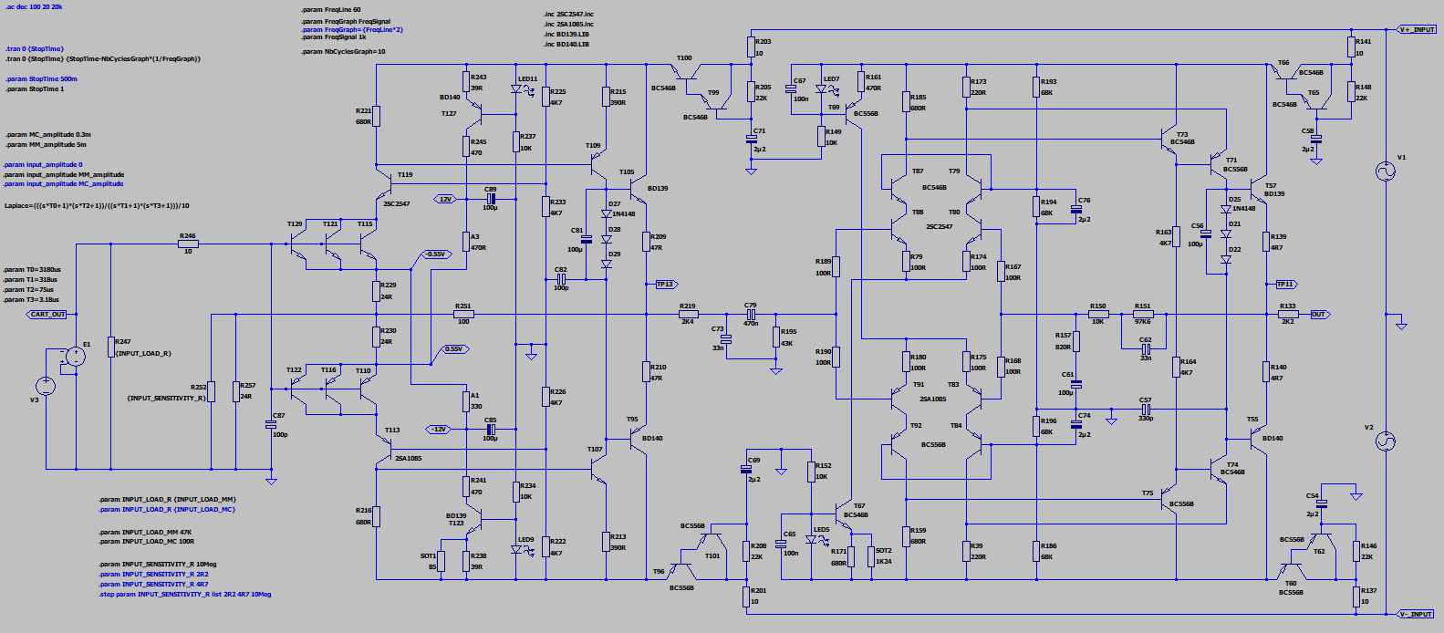
Here's some more observations from analysing the schematic. I think I'm getting there but pardon my ignorance 🤔. There are some unresolved questions and bugs (see below). I have put the necessary files in the attached zip archive if you want to play with the design in LTspice.
BUGS.
More questions.
1. What is the purpose of resistor R257 (24R) between the input transistor emitter resistors and ground?
2. What is the purpose of the snubber formed by resistor R157 (820R) and capacitor C61 (100uF)?
3. There is the possibility of DC offset at the output. In the integrated amplifier this circuit feeds through R133 (2K2) into a 1uF capacitor followed by a 50K audio potentiometer; In the context of a standalone version, can this resistor be dropped or reduced, leaving the responsability of DC blocking to the subsequent component, or should the project integrate an output capacitor at the risk of double series capacitors?
- R251 (100R) provides feedback from the first stage output (TP13) to the input stage transistors.
- SOT1 is critical for output gain. Going from 85 to 1meg, gain at TP11 fell from mostly flat around 37dB (normal) to about 14dB below 1 KHZ and down to 10dB at 20kHz. Adjusting this resistor is one of the factors determining the current through the input transistors, along with the value of emitter resistors R229 and R230.
- In the simulation I was able to match the specified 2V drop across the 680 ohm collector resistors and the 1.5V drop across the 390R gain stage emitter resistors with a 85 Ohm SOT resistor but at the expense of overshooting the voltage between resistors R241 and A1 to -16V instead of the -12V specified on the original schematic. To restore equal DC operating points on each side of the Ax resistors (11.4V in my simulation) I reduced the value of the lower A1 resistor to 330R. Is that a proper approach or is the +-12V operating points being equal is not that important, it is the value of A1 and A3 that needs be matched?
- Of course the currents through the two opposing sources are unequal now, I guess that's okay since the circuit is built with this S.O.T. resistor parallel to the lower current source setting resistor.
- The current through the current source is very sensitive to the value of SOT1; it had to be adjusted in 1 ohm increments.
- The gain of the first stage at TP13 is 32.8 dB;
- The 75uS low-pass passive filter attenuates up to 20dB at 20 KHz.
- The 470nF coupling capacitor to the second stage with the 43K is a high-pass filter that rolls off frequencies below 20Hz.
- The current mirror implementation and the constant current sinks set an identical DC operating point for the two second stage cascodes.
- The feedback network between the second cascode and the final gain section implements 318us/3180us RIAA equalization through the low-pass filter C62/R151/R150.
- The AC gain of the second stage cascode (after 75uS passive filtering of the first stage) is set by the load resistors and output load: Av.Vin.(RL/(RL + Rout), and reduced below the 318uS zero by the feedback network.
- The first differential cascode output drives the level shifter formed by T73 and T75 (28 uA base current each).
- The second differential cascode shares its load resistor with transistors T71 and T74 emitters (2.5 mA); this performs the RIAA LF boost through degenerative feedback, as more feedback is fed at high frequencies from the cascode's gain spectrum.
- SOT2 has an effect on the DC offset present at TP11.
BUGS.
- I am unable to get to the .95V and .75V operating points of the second stage unless by using a different LED model (L128-FRD1003500000) than the one used in the first stage's current sources. I doubt there are two different LED models in the actual design...
- Unable to get both 0.75V voltages equal at the output of the cascodes... going to set SOT2 for an average of 0.75V between the two. Need to tweak the load resistors?
- Unable to get to the .34V (getting 79mV with the specified 47R) across final emitter resistors R139 and R140 unless they are raised to 22K ! ! That can't be right... From the schematic it is evident that the two .34V voltage drops plus the two output transistors' Vbe has to be equal to the voltage drop across the three bias diodes... Not enough gain?
More questions.
1. What is the purpose of resistor R257 (24R) between the input transistor emitter resistors and ground?
2. What is the purpose of the snubber formed by resistor R157 (820R) and capacitor C61 (100uF)?
3. There is the possibility of DC offset at the output. In the integrated amplifier this circuit feeds through R133 (2K2) into a 1uF capacitor followed by a 50K audio potentiometer; In the context of a standalone version, can this resistor be dropped or reduced, leaving the responsability of DC blocking to the subsequent component, or should the project integrate an output capacitor at the risk of double series capacitors?
Attachments
Partial answer:
1. It's part of the feedback network of the first stage (like in a non-inverting amplifier with an op-amp).
2. Part of the feedback network of the second stage. The series capacitor limits the DC voltage gain to unity, presumably because the offset voltage at the output could otherwise become excessively large.
Marcel I appreciate very much you accompany me in my exploration.
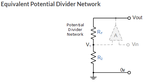
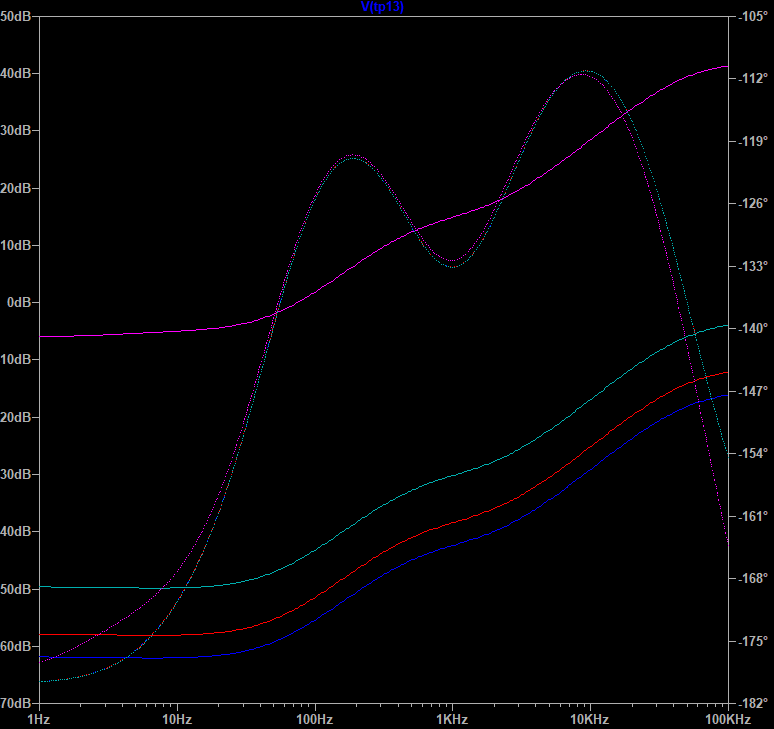
If I understand the analogy with the non-inverting operational amplifier configuration, resistor R257 (24R) between the input transistor emitter resistors and ground is the equivalent of the resistor from the inverting input to ground in non-inverting operational amplifier configuration, e.g. the lower arm of the equivalent potential divider with the upper arm being the 100R R251 resistor. The insertion of parallel "sensitivity" resistors R252 and R257 through the DIP switches increase the feedback ratio and consequently gain. This is the case at the output of the cascode (1st graph - the close lines represent 4R7, 2R2, and the parallel equivalent 1R5 of these two). But the output of the cascode is inverted by the emitter follower drivers so the gain is actually lower at the output of the 1st gain stage (TP13, 2nd graph). So I'm a bit lost on the role of the sensitivity resistors.
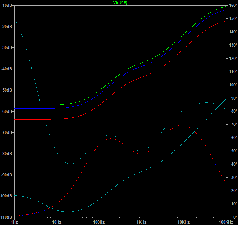
On the second stage, resistor R157 (820R) and capacitor C61 (100uF) form a low-pass filter of 1.94 Hz corner frequency. It is the equivalent of the lower arm of the equivalent gain potential divider with the upper arm being the 318us/3180us RIAA equalization through the low-pass filter C62/R151/R150. So as the feedback network present a low output impedance towards DC, the feedback ratio raises and so is the gain but this too is fed as an inverted signal to the final driver emitter followers so in the end gain ends up reduced at very low frequencies near DC. This is verified on the AC simulation.
If I understand the analogy with the non-inverting operational amplifier configuration, resistor R257 (24R) between the input transistor emitter resistors and ground is the equivalent of the resistor from the inverting input to ground in non-inverting operational amplifier configuration, e.g. the lower arm of the equivalent potential divider with the upper arm being the 100R R251 resistor. The insertion of parallel "sensitivity" resistors R252 and R257 through the DIP switches increase the feedback ratio and consequently gain. This is the case at the output of the cascode (1st graph - the close lines represent 4R7, 2R2, and the parallel equivalent 1R5 of these two). But the output of the cascode is inverted by the emitter follower drivers so the gain is actually lower at the output of the 1st gain stage (TP13, 2nd graph). So I'm a bit lost on the role of the sensitivity resistors.
On the second stage, resistor R157 (820R) and capacitor C61 (100uF) form a low-pass filter of 1.94 Hz corner frequency. It is the equivalent of the lower arm of the equivalent gain potential divider with the upper arm being the 318us/3180us RIAA equalization through the low-pass filter C62/R151/R150. So as the feedback network present a low output impedance towards DC, the feedback ratio raises and so is the gain but this too is fed as an inverted signal to the final driver emitter followers so in the end gain ends up reduced at very low frequencies near DC. This is verified on the AC simulation.
Disregard my last comments regarding sensitivity resistors, I don't know what I did wrong but looking at the graphs now everything makes sense. At the last stage output (TP11) the gain range from 40dB for MM to 60dB for the last very high input feedback ratio MC setting. In my case, that last setting was a bit too noisy; with my Denon DL-103 I'm running it with the 4R7 sensitivity resistor only, which in the simulation gives 50dB gain.
I'm practically done with my low-voltage clone integrating Marcel's earlier suggestions in this thread, with lower total input collector currents and Vbe-based current sources. Schematics soon!
I'm practically done with my low-voltage clone integrating Marcel's earlier suggestions in this thread, with lower total input collector currents and Vbe-based current sources. Schematics soon!
So here is my low voltage version running on +-15V supply instead of the +-40V of the original design. With respect to the original schematic, the modifications essentially boil down to lowering resistor values to maintain the same currents as the original design and adjusting associated filter capacitors where applicable. The necessary LTspice files are in the zip archive below if you want to play with the simulation.
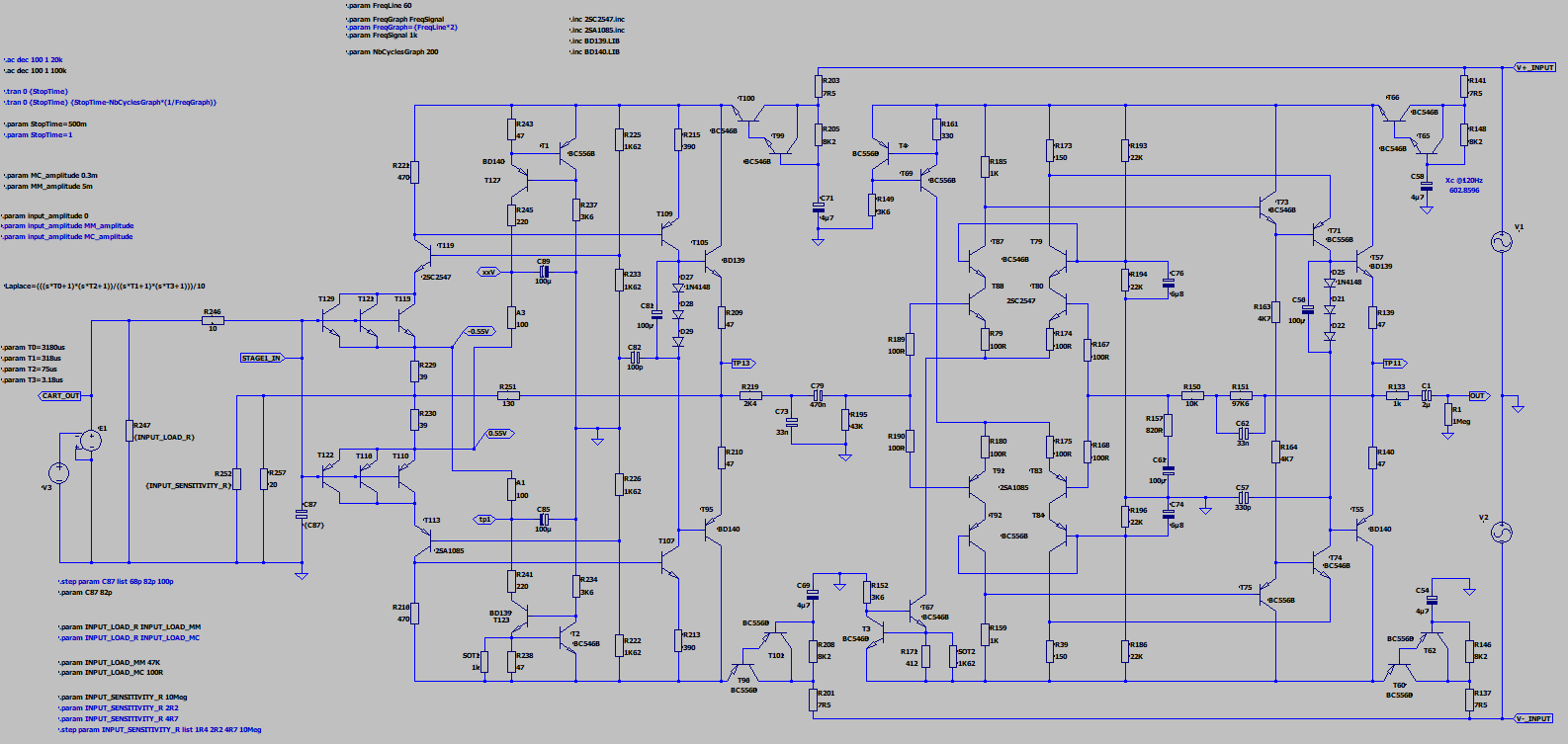
Notes and modifications done to the original design:
General notes
---------------
- Part references apply to the right channel schematic of the original ISS3 schematics.
1. Modifications applied on both stages
2. Modifications applied on first stage
- Modifications done in accordance with Marcel's recommendation from post #39 :
- Replaced LED referenced current sources with Vbe-based ones
- Increased input emitter resistors from 24R to 39R;
- Increased input cascode collector loads to reduce total input stage current to around 1 mA total for all six transistors;
3. Modifications applied on second stage
The input stages being cascode they have a high output impedance so they are followed by emitter followers before the final gain stages; So I kept emitter follower degeneration resistors values as is to present the same input impedance to the previous cascodes.
Lastly I added a big output coupling cap and resistor.
4. Possible modifications
As always all comments are welcome. Thanks to all you helped me a lot!
Joris
Notes and modifications done to the original design:
General notes
---------------
- Part references apply to the right channel schematic of the original ISS3 schematics.
1. Modifications applied on both stages
- Decreased power supply feed resistors from 10R to 7R5 for a bit more headroom;
- Decreased power supply low-pass filter resistors from 22K to 8K2 to maintain same base current for the Darlington pairs; Low-pass filter capacitors adjusted accordingly from 2u2 to 4u7 to maintain same f-3dB (around 603 Hz);
- Decreased current source BJT reference transistor feed resistors from 10K to 3K6 to maintain same current through them as the LED references of the original design;
2. Modifications applied on first stage
- Modifications done in accordance with Marcel's recommendation from post #39 :
- Replaced LED referenced current sources with Vbe-based ones
- Increased input emitter resistors from 24R to 39R;
- Increased input cascode collector loads to reduce total input stage current to around 1 mA total for all six transistors;
- Increased feedback ratio a bit : R257 reduced from 24R to 20R, R251 Increased from 100R to 130R; this should give a bit more gain for the first stage.
- Increased input sensitivity resistor R252 from 2R2 to 2R7 to maintain about the same feedback ratio (hence gain) as before since that last position has too much gain and is too noisy in the original amp; The 2R7 gives a little bit less gain at the extreme sensitivity setting.
3. Modifications applied on second stage
- Decreased second stage cascodes bias resistors from 68K to 22K to maintain about the same base current (282uA against 313uA through R193 - A 27K would be closer but I don't have any); Low-pass filter capacitors adjusted accordingly from 2u2 to 6u8 to maintain same f-3dB (2.13 Hz); Note that I used the paralleled value of R193/R194 and R186/R196 for the filter calculation as they are conected together through the low impedance of the power supply.
- Increased second stage input cascode collector loads and decreased second stage active feedback cascode collector loads by the same ratio for a bit more gain; The second cascode gain needs to be reduced because the active feedback signal is inverted at the output to provide RIAA LF boost;
- Reduced output series resistor R133 from 2K2 to 1K to allow more output drive.
The input stages being cascode they have a high output impedance so they are followed by emitter followers before the final gain stages; So I kept emitter follower degeneration resistors values as is to present the same input impedance to the previous cascodes.
Lastly I added a big output coupling cap and resistor.
4. Possible modifications
- Eq capacitors actual value is 33.2nF, should R150 be decreased from 10K to 9K6? ( T4 goes nearer to the required zero (499.6Hz for 9K6 instead of 479.6Hz for 10K).
- Increase current to the second stage bias network voltage divider to reduce the influence of variations in base current through the second cascode gain stage
- Replace discrete Darlington configurations by monolithic parts.
As always all comments are welcome. Thanks to all you helped me a lot!
Joris
Attachments
Hello Ed,
Can we elaborate on this? I have simulated the MC setting I use with values for the last output resistor to match the impedance of a 50K volume pot in parallel with the 1Meg, also the input impedance of my digital recorder (10k//1Meg) and when loaded with both (1Meg//25k//10k). All in all the loss at maximum load is -1.17dB with respect to the 1Meg output resistor alone (pink trace). That doesn't seem too bad no? That is why I tried to stretch a bit more gain than the original design.
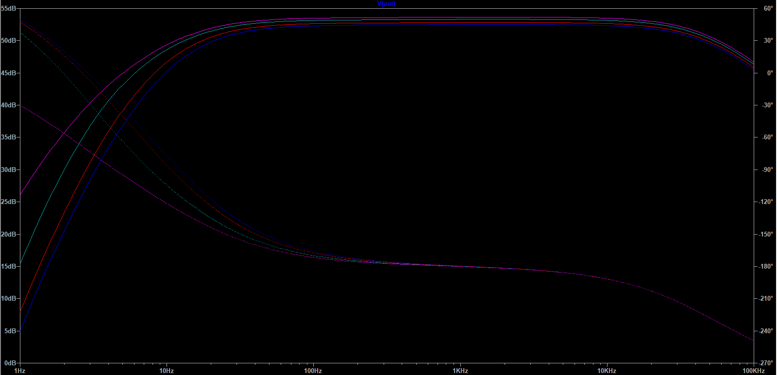
Of course the LF roll-off is more pronounced at higher load, I guess that is why you would recommend more output capacitance. If I want a larger output capacitor value I may have to go off-board but that's feasible.
The 2uF output capacitor is too small
Can we elaborate on this? I have simulated the MC setting I use with values for the last output resistor to match the impedance of a 50K volume pot in parallel with the 1Meg, also the input impedance of my digital recorder (10k//1Meg) and when loaded with both (1Meg//25k//10k). All in all the loss at maximum load is -1.17dB with respect to the 1Meg output resistor alone (pink trace). That doesn't seem too bad no? That is why I tried to stretch a bit more gain than the original design.
Of course the LF roll-off is more pronounced at higher load, I guess that is why you would recommend more output capacitance. If I want a larger output capacitor value I may have to go off-board but that's feasible.
The output capacitor can easily be made large enough not to have any effect on the frequency response. The circuit already has a 100uF electrolytic for the second op-amp's DC feedback. Why not use another?
Direct coupling is even better. The offset should be millivolts.
Ed
Direct coupling is even better. The offset should be millivolts.
Ed
I'd like to avoid electrolytics in the audio path (except for DC blocking). But I guess could do a lytic or largish polyester bypassed with a smaller better cap like polystyrene or teflon film like I saw in some designs.Why not use another?
As a matter of fact I'm thinking of having a direct coupling switch across the output cap but I still have questions regarding that. Does a typical audio component tolerate more than a few millivolts DC at its input? Can the output stage DC drift with time? I am not very knowledgeable of the various physical parameters in play in transistors, most notably heat, and their effects on DC drift in a complementary push-pull design like this. The degenerative feedback provided by the emitter resistors probably help for thermal stability though.Direct coupling is even better. The offset should be millivolts.
Thanks for your reply, I appreciate your input.
Yes, bypass the electrolytic with a smaller capacitor. Do that for the DC feedback electrolytic as well.
BTW, I use direct coupling in my pre-amp.
The offset will mainly be due to the base current across the 43K and 97.6K resistors. That could be 100mV. I don't think that would trip up any equipment, but it is a bit high.
Ed
BTW, I use direct coupling in my pre-amp.
The offset will mainly be due to the base current across the 43K and 97.6K resistors. That could be 100mV. I don't think that would trip up any equipment, but it is a bit high.
Ed
Just to be clear, are we are talking about the 100uFs across the bias diodes ?Do that for the DC feedback electrolytic as well.
- Home
- Design & Build
- Electronic Design
- Understanding this MM/MC discrete phono stage
