Not sure if I’m asking in the right place but here goes. I frequently replace TO3 and MT200 output devices with TO3p and TO247/TO264. Generally, the only complaint about doing this would be the smaller heat spreader. I was trying to figure out how to get around this, thinking of making aluminum plates, the same shape as the original devices, but I’m still at the mercy of the thermal compound then I saw a product on xraytonyb’s channel and realized it was exactly what I was looking for. Instead of using aluminum, I would use copper and then solder the device directly to that plate. This product was developed by Hoppe’s brain.
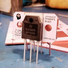
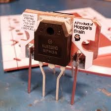
This method is likely the best you were going to get to replacing the larger heat spreader. As soon as I saw it, I was thinking of also making them for TO3 and the batwing transistors using TO220. wouldn’t you know I found that he was also developing those. So instead of buying a sheet of copper and cutting them out myself I figured that since JLCPCB offers boards that use a solid copper substrate I could have them do it. Basically, I would be ordering boards with no traces on them, I don’t even have to have a silk screen. I would be completely happy with just copper cut outs.
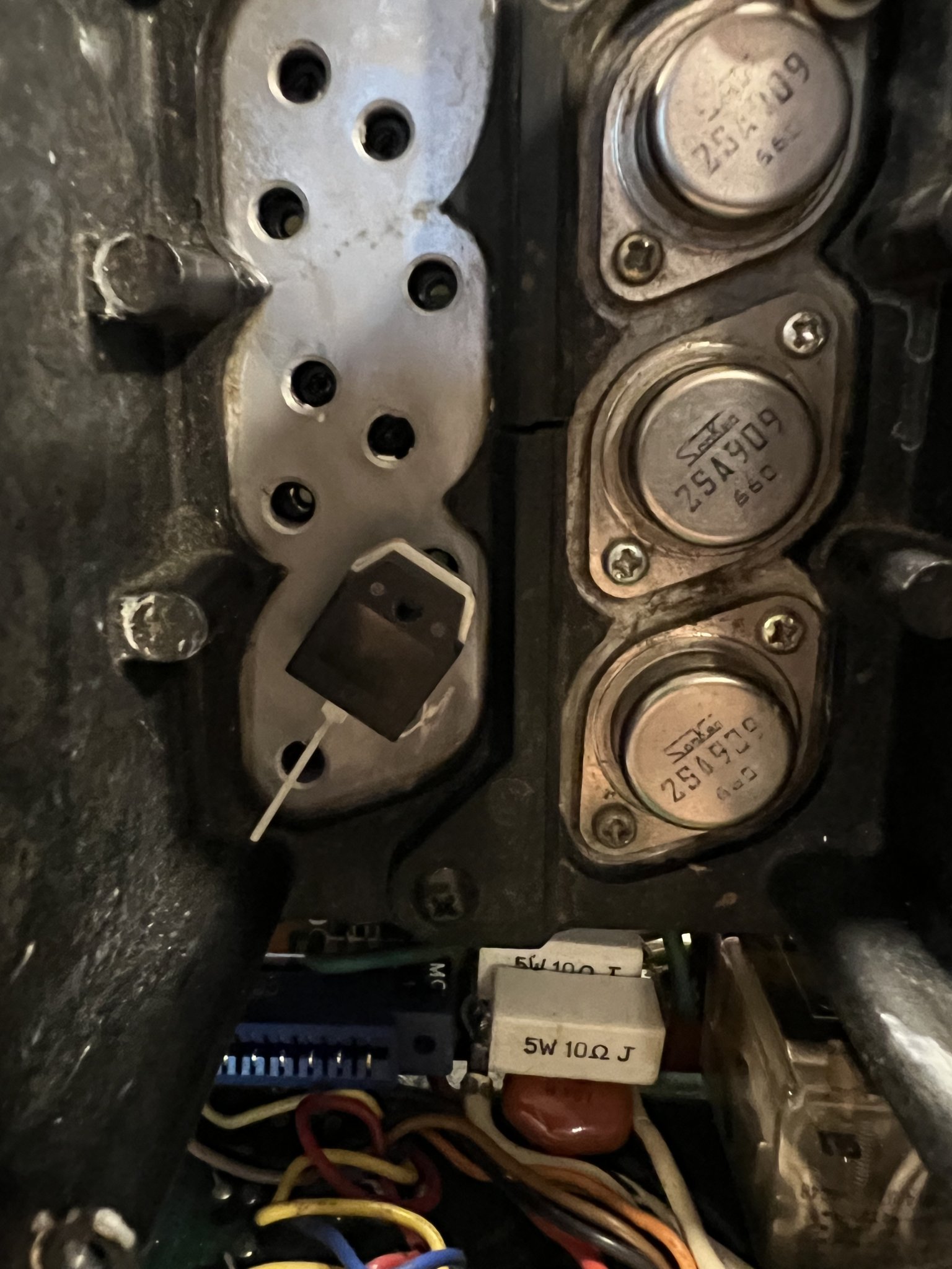
I am replacing some right now and they would definitely be handy. I would buy them directly from Hoppe’s, but I use these frequently enough that I would like to purchase around 100 of each shape and ordering them from him would be very costly. So to make these files and send them to JLCPCB would Kicad be the best option? I don’t know what the best/ cheapest solution would be have them cut out all the shapes individually or have them ship me aboard where I clip them out myself with a pair of snips, meaning have like 20 to a sheet that I cut out on my own. Just looking for guidance really.
If there is anyone that would be interested in doing up the Gerber files in exchange for some of the plates, I would be very interested in that as well, I don’t have a lot of experience doing this type of thing. I’m thinking that since the drawing is one dimension, basically like a cookie cutter that it wouldn’t be too difficult to do the file, but I don’t know.
Thank you,
Dan
This method is likely the best you were going to get to replacing the larger heat spreader. As soon as I saw it, I was thinking of also making them for TO3 and the batwing transistors using TO220. wouldn’t you know I found that he was also developing those. So instead of buying a sheet of copper and cutting them out myself I figured that since JLCPCB offers boards that use a solid copper substrate I could have them do it. Basically, I would be ordering boards with no traces on them, I don’t even have to have a silk screen. I would be completely happy with just copper cut outs.
I am replacing some right now and they would definitely be handy. I would buy them directly from Hoppe’s, but I use these frequently enough that I would like to purchase around 100 of each shape and ordering them from him would be very costly. So to make these files and send them to JLCPCB would Kicad be the best option? I don’t know what the best/ cheapest solution would be have them cut out all the shapes individually or have them ship me aboard where I clip them out myself with a pair of snips, meaning have like 20 to a sheet that I cut out on my own. Just looking for guidance really.
If there is anyone that would be interested in doing up the Gerber files in exchange for some of the plates, I would be very interested in that as well, I don’t have a lot of experience doing this type of thing. I’m thinking that since the drawing is one dimension, basically like a cookie cutter that it wouldn’t be too difficult to do the file, but I don’t know.
Thank you,
Dan
The best pcb program is the one you already know how to use. Simple boards like this can be done by any such program.
But the copper won't be very thick, probably 2 oz. except for much more expensive boards. Some make up to 10 oz boards.
You don't want to be cutting the boards apart yourself when the pcb house will do it for you.
But soldering the devices to the pcb may be more difficult than you think.
But the copper won't be very thick, probably 2 oz. except for much more expensive boards. Some make up to 10 oz boards.
You don't want to be cutting the boards apart yourself when the pcb house will do it for you.
But soldering the devices to the pcb may be more difficult than you think.
Last edited:
Yes, you can have solid copper pieces made instead. You would need .dxf files, not pcb files.
These guys make laser cut metal pieces inexpensively. Of course, solid copper is not cheap.
And soldering the device to the thick copper would be even more difficult.
https://sendcutsend.com/
These guys make laser cut metal pieces inexpensively. Of course, solid copper is not cheap.
And soldering the device to the thick copper would be even more difficult.
https://sendcutsend.com/
Job for a temperature-controlled hotplate I think...And soldering the device to the thick copper would be even more difficult.
Where else is there but the USA? Isn’t it the center of the universe?Only in the USA, these guys are pretty provincial.
jan
Sorry still behind the times, just feel like it is still the first.
Wow Ed, so sensitive!
As you probably know, there's about 24 other persons for each american.
Of course you may counter that that only proves an american is worth 24 other persons, but that will get us into the forbidden political arena 😎
Jan
As you probably know, there's about 24 other persons for each american.
Of course you may counter that that only proves an american is worth 24 other persons, but that will get us into the forbidden political arena 😎
Jan
Sendcutsend pays all US shipping, which is too expensive for international shipments of heavy metal pieces.
Canada shipping is at a flat $19. per order.
Canada shipping is at a flat $19. per order.
I think to be useful that copper backplate must be at least 1.5 or 2 mm thick, which I guess is well beyond any PCB fabrication house.
One problem with cutting sheet metal, specially a malleable one such as copper, is that it will lose flatness, which is essential for your purpose.
Shear "knives" will twist it into a spiral ribbon.
Admittedly, very little, but enough to be a nuisance, a commercial metal shop will either pass them through rollers or stamp them between two flat surface dies.
You can cut them oversize and then shear away edges, so center piece stays flat and edges twist like ADN ribbons.
I would ask a metallurgical shop for suggestions, not a PCB one.
Plan B: you can "chemically machine" your copper parts.
You silkscreen slightly oversize rectangles using etch-resist ink/paint and then drop parts in an acid etch bath.
Commonly done for small parts, not so sure on such thick ones but you might try.
To experiment, just brush a rectangle on both sides of a copper plate and drop it in an etch tank (perchloride or similar), it will easily take overnight but hey.
https://ppdltd.com/the-process.html
It is essentially same process as PCB making, but here they are focused on "thick" metal plates, these are not just one thin layer in a complex PCB.
Some places make PCBs with thick copper or aluminium backplates. Much thicker than any 10 oz. Intended as a ground plane and heat sink for RF devices. Tends to be pricey - and often you have to supply the material. Yep, you can buy it. Again, pricey. I’m sure it’s a lot less with FR4, but my experience is mostly with Rogers PTFE.The best pcb program is the one you already know how to use. Simple boards like this can be done by any such program.
But the copper won't be very thick, probably 2 oz. except for much more expensive boards. Some make up to 10 oz boards.
You don't want to be cutting the boards apart yourself when the pcb house will do it for you.
But soldering the devices to the pcb may be more difficult than you think.
Soldering requires a vacuum reflow chamber, in order to do it right. Voiding is an issue. Also the CTE mismatch needs to be managed - it affects how much thermal cycling it can take before Rth starts climbing. And it will.
There is also aluminium cored PCB (a.k.a IMS), a single sided PCB for surface mount with great heat-sinking ability. This is why you can now get SMT wire-links for hopping over other traces.
Jan,Wow Ed, so sensitive!
As you probably know, there's about 24 other persons for each american.
Of course you may counter that that only proves an american is worth 24 other persons, but that will get us into the forbidden political arena 😎
Jan
Everywhere I go, all I see is Americans! Although there are some politicians who warn about about other folks they call aliens, but I have yet to see a flying saucer!
Just a thought regarding alternatives. A cheap hydraulic press (Harbor Freight perhaps) and a punch die made by a local machine shop or other would be pretty convenient and easy.
Nothing, of course, is as convenient as loading a file, entering a quantity and pressing the place order button, especially if the pieces are delivered dressed with clean edges.
Nothing, of course, is as convenient as loading a file, entering a quantity and pressing the place order button, especially if the pieces are delivered dressed with clean edges.
My adapter plates are made by JLCPCB, and they're 1.6mm thick, exactly the same as an MT-200. Higher-power-rated MT-200's are actually TO-3P heat-spreaders soldered to another, larger heat-spreader.
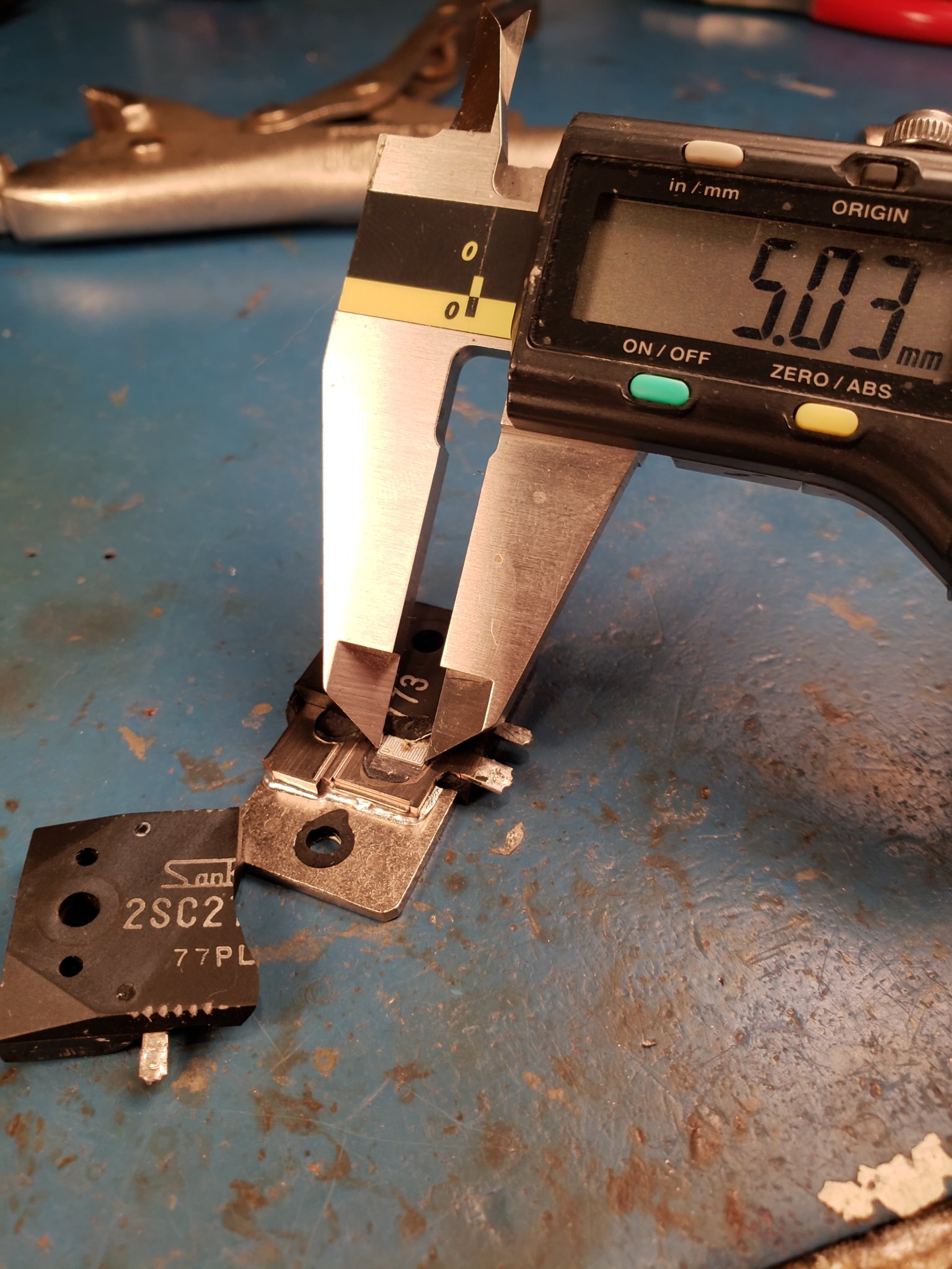
The adapters are "direct copper heatsink" PCB technology, so they are solid copper all the way through.
Voiding is prevented by applying pressure as the solder-paste melts. The alligator clips press the transistor flat against the substrate.
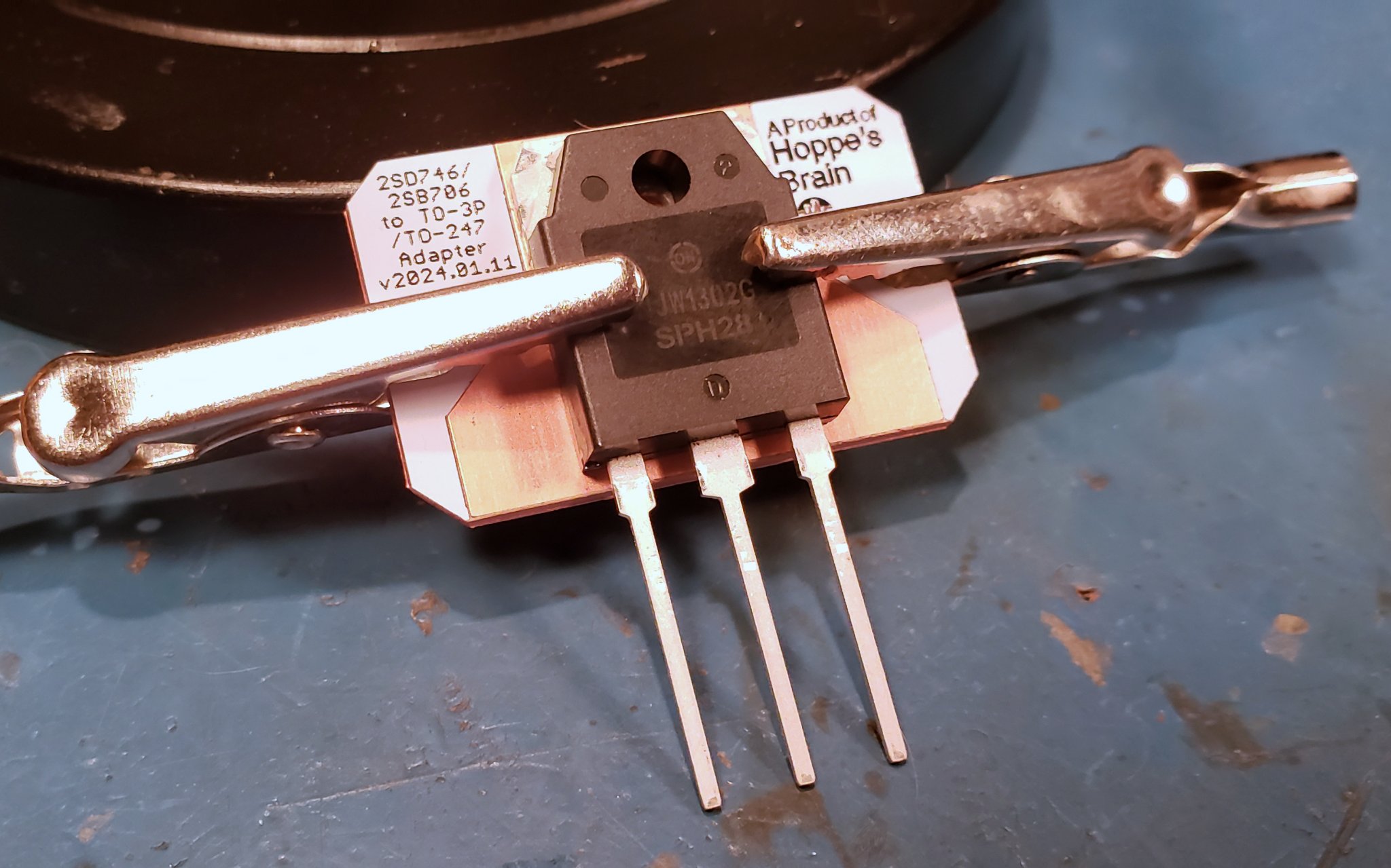
Voids are squeezed out along with a small amount of excess solder. I cut and polished one at a shallow angle and found no voids, and the layer of solder is super thin but contiguous.
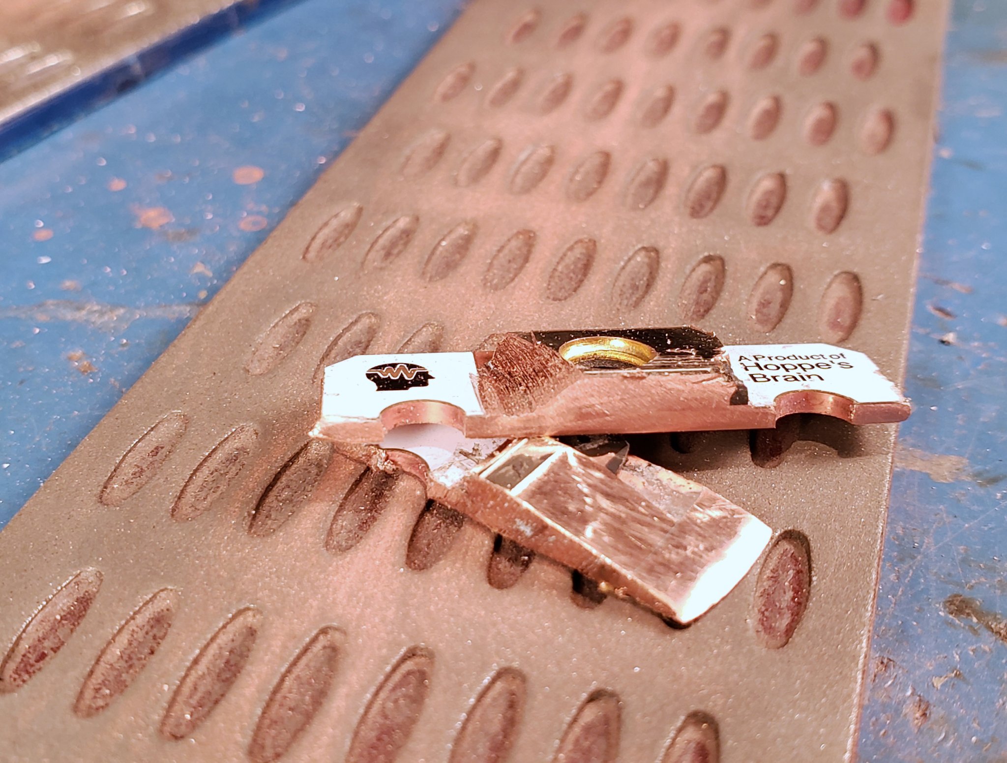
I think they're reasonably priced. As simple as they are, I've been working on this projects for weeks and weeks... reading datasheets, researching different types of obscure semiconductor packages, performing thermal testing, researching mounting methods, and writing documentation.
There is a volume discount, and it you need that many we can work something out.
The adapters are "direct copper heatsink" PCB technology, so they are solid copper all the way through.
Voiding is prevented by applying pressure as the solder-paste melts. The alligator clips press the transistor flat against the substrate.
Voids are squeezed out along with a small amount of excess solder. I cut and polished one at a shallow angle and found no voids, and the layer of solder is super thin but contiguous.
I think they're reasonably priced. As simple as they are, I've been working on this projects for weeks and weeks... reading datasheets, researching different types of obscure semiconductor packages, performing thermal testing, researching mounting methods, and writing documentation.
There is a volume discount, and it you need that many we can work something out.
Actually, the soldering goes super easy, (hot air) much easier than with a fiberglass PCB, because the copper conducts heat so well and the whole surface of the adapter heats up evenly. Once it melts, it all goes at once. Remove heat as the moment that happens and you'be be easily inside the thermal profile; most transistors specify a maximum die to case temperature of 260C for 5 seconds. Eutectic solder melts at 183C.
Last edited:
Aluminum substrate PCBs are not very expensive. I've ordered some for power JFETs from JLCPCB.
A nice thing about these metal PCBs is that the top copper layer is insulated from the metal substrate with a dielectric layer, so an insulator may not be needed between the PCB and the heatsink. This is easily done for surface mount transistors, although for through-hole devices, care needs to be taken with the board layout.
A nice thing about these metal PCBs is that the top copper layer is insulated from the metal substrate with a dielectric layer, so an insulator may not be needed between the PCB and the heatsink. This is easily done for surface mount transistors, although for through-hole devices, care needs to be taken with the board layout.
Attachments
Indeed, Rockford Fosgate did this with a bunch of power amplifiers with reliable results. They mounted two output transistors side by side on an aluminum PCB, with the PCB just screwed to the heatsink, no pad, just thermal paste. It has a lot of advantages. Thermal pads aren't cheap. The aluminum-oxide insulating layer probably performs better than a thermal pad, and it's very very thin. It eliminates of complicated mounting hardware... All those bar-clamps and stuff are fussy to install at the factory. More manual labor than just screwing this assembly to the heatsink. And the bar-clamps look pretty meh, the amp is going to look way cooler inside with the transistors uncovered, and that actually matters to car audio nuts. And there is no physical pressure on the transistor! This could all be done with a copper-core PCB instead, and wow that would perform amazing.
I had thought about making the MT-200 adapters this way, so you wouldn't need a thermal pad, but decided against it. The insulating layer would hamper the heat-spreading ability of the copper, and overall the performance would suffer versus a real MT-200. It would be more prone to a hot-spot on the die under pulse conditions, it wouldn't clear the heat away as fast.
I had thought about making the MT-200 adapters this way, so you wouldn't need a thermal pad, but decided against it. The insulating layer would hamper the heat-spreading ability of the copper, and overall the performance would suffer versus a real MT-200. It would be more prone to a hot-spot on the die under pulse conditions, it wouldn't clear the heat away as fast.
Just found this article from Rockford Fosgate describing it, their marketing buzzword for it is MEHSA technology, Maximum Efficiency Heat Sink Application, 🙄 OK
It is a good idea. Done in copper, even better.
It is a good idea. Done in copper, even better.
- Home
- Design & Build
- Parts
- Wanting to order very simple parts from JLCPCB, do I need Kicad for these?
