ON has real good matching right out of the tube.
My 3 pair tester amp was "cooked" overnight with .15R @ over 60C.
less than a mV difference between the pairs.
My other 3 .22R 5-pair amps have been run for 7 months now - no issue.
Then the hundreds of other 5 pair amps with .22R and 4.7R stoppers - not
one failure.
If alan is actually matching the ON's , I know at 60-100ma - no issues.
200+ , I don't do that .... who knows.
With my Sanken MT-200's , I ran >250ma just to see how hardy the
devices were. I really let it cook overnight ... actually warmed my
little "workcloset' right up ! Re's all tested the same Vdrop from 20-70C.
That one also has 4.7R stoppers and .22 Re's.
Sanken MT-100's are quite poorly matched , always check them. The 200's
also fall far short of the ON's.
I actually tried to let "magic smoke" out of the Sanken's - Nope , even
at almost 500ma per device. Never saw Waly's scenario - even running a
signal into a load (with the overbias).
OS
You guys are again killing my sleep
") .
.Obviously 0.22 ohm with 4.7 ohm base stoppers are certainly good for matched output devices. 0.1 ohm for 5 pairs, it's way to risky to even consider. Current hogging is the problem, not static cooking even at high bias. Usually the disaster starts because of the temperature gradient on the heat sink.
Hi Alan,
Your safe dissipation depends on many factors, the most basic being thermal resistance to the air. This can change a negative tempco to a positive one.
Beta matching is the critical issue with both output transistors (and drivers) and the differential pair(s). Vbe is never far off and a few mV will not change things significantly.
Offsetting the crossover point is totally different than increasing the bias current for reasons Forr, Waly and Ostripper have discussed.
I think you are missing some points purely due to your insistence that everything Doug Self has written is incorrect. I have books from both Bob and Doug, and they both have great value. I enjoyed reading both. If you can't look at both perspectives, it is you that loses out.
For my part I found it to be very uncomfortable to watch you attack Mr. Self's work at every opportunity. Many other people may have felt the same. What you really need to be able to do is have another read of Doug Self's book with an open mind. The same holds true for Bob Cordell's book. I'm pretty certain that Bob does not want anyone to blindly accept what he has written.
-Chris
Also bear in mind that base stopper resistors (divided by Beta) are to be subtracted from the emitter resistors, to find out the effective value. Internal emitter resistance (bond wire and emitter diffusion resistance, to the EB junction) adds to the external emitter resistor.
Why is base stopper/beta has to be subtracted from the value of emitter resistor?
with 5 pairs, use 0.47 ohm no problems what so ever
I am trying to satisfy the Oliver's condition of using Re with value that drop 26mV with the idle current. If I run 200mA, I need 0.13ohm. I can only get 0.12ohm. with the resistance of the bonding wires inside the transistor, that should give me 0.13ohm.
I am at the process also in buying a lower voltage transformer to get only +/-25 to +/-28V rails to lower the power dissipation of the transistors and even up the current to 250mA. The 0.12ohm resistor should be perfect to get 26mV across.
Increase to higher resistance will violate the Oliver's condition and cause more crossover distortion.
There is no difference with heavy idle current that you displace the kink of the curve away from the center. How far you move the kinked area depends on how much idle current you have. This is exactly the same whether you use a CCS to pull in the Self XD or just simply run higher idle current. There is absolutely no difference in the displacement of the kink.
.
This is not correct. Even with full class A biasing, the 'kink' (however small) is still smack in the middle of the transfer curve.
There are many of these curves as a function of Re and Ibias in both Douglas' and Bob's book, and they all show that.
See, for example, attached 'kink': when you inclease Ibias, the kink gets smoothed out but does not move from center. Viewed from another dimension, it closely mimics the so called 'wingspread' plots. They may vary in shape but are always symmetrical around zero (assuming complemetary output stage).
Jan
Attachments
Last edited:
This is not correct. Even with full class A biasing, the 'kink' (however small) is still smack in the middle of the transfer curve.
There are many of these curves as a function of Re and Ibias in both Douglas' and Bob's book,and they all show that.
See, for example, attached 'kink': when you inclease Ibias, the kink gets smoothed out but does not move from center. Viewed from another dimension, it closely mimics the so called 'wingspread' plots. They may vary in shape but are always symmetrical around zero (assuming complemetary output stage).
Jan
Don't think the response of the XD is flat at the center. You pull current with the CCS, when you drive a load, the current through the top NPN is going to vary from the CCS current to zero when move from the center to the offset kink. If the CCS is pulling 1A, the NPN current vary between 1A to 0 just moving from the center to the kink. r'e change big from 26mohm to infinity( say some high value) during the transition. This alone will create distortion. remember, the PNP EF is off with the CCS as long as the load current does not exceed the sinking capability of the CCS.
Back to just the kink, I am talking about using higher current. Of cause if you bias with 50mA idle, the kink is very close to the center and severe as show in Fig.10.31. BUT if you bias at over 200mA, the middle is a lot broader and smoother as shown. ALSO, the worst part of the kink is beyond the kink of the XD for the same bias current. There is no other way about this.
If I want 10W of class A into 4ohm, I bias 5 stages to 220mA each, I avoid most of the kink in the normal listening level. BUT if I run XD, the bias has to be DOUBLE to move the kink as far.
In another words, if you set the CCS of the XD to low current like 100mA, you are not moving the kink much off the center. You easily hit the crossover and you get distortion. You will have to set the CCS to 400mA in order to move the kink as far as if I set the Class AB to 200mA.
If you use 5 stages like me, you'll almost never hit the worst part of the kink with total bias current of 1A to 1.5A. To match this with XD, you are going to have the CCS to pull 2A to 3A respectively.
Last edited:
to be fair the thermal response will be an effect in real amps, is poorly (not at all) dealt with in Spice - have to add your own thermal models and coupling to transistor parameters
This is exactly right.
Cheers,
Bob
Don't think the response of the XD is flat at the center. You pull current with the CCS, when you drive a load, the current through the top NPN is going to vary from the CCS current to zero when move from the center to the offset kink. If the CCS is pulling 1A, the NPN current vary between 1A to 0 just moving from the center to the kink. r'e change big from 26mohm to infinity( say some high value) during the transition. This alone will create distortion. remember, the PNP EF is off with the CCS as long as the load current does not exceed the sinking capability of the CCS.
Back to just the kink, I am talking about using higher current. Of cause if you bias with 50mA idle, the kink is very close to the center and severe as show in Fig.10.31. BUT if you bias at over 200mA, the middle is a lot broader and smoother as shown. ALSO, the worst part of the kink is beyond the kink of the XD for the same bias current. There is no other way about this.
If I want 10W of class A into 4ohm, I bias 5 stages to 220mA each, I avoid most of the kink in the normal listening level. BUT if I run XD, the bias has to be DOUBLE to move the kink as far.
In another words, if you set the CCS of the XD to low current like 100mA, you are not moving the kink much off the center. You easily hit the crossover and you get distortion. You will have to set the CCS to 400mA in order to move the kink as far as if I set the Class AB to 200mA.
If you use 5 stages like me, you'll almost never hit the worst part of the kink with total bias current of 1A to 1.5A. To match this with XD, you are going to have the CCS to pull 2A to 3A respectively.
Alan I think we don't disagree. I took exception to your statement that Ibias can move the kink off-center but probably you meant XD - agreed. Not so for 'regular class A/AB/A of course.
In XD, the CCS sets how far the kink moves off-center and thus how far the output can go in class A before moving into AB territory. This is also the case in regular class AB. In regular AB the class A area is around the center, with two devices involved; with XD the class A area has only one device involved. I don't know what the difference on performance would be. For instance, is there a difference in 'Gm doubling' in the two cases?
Where's Douglas when you need him? ;-)
Edit: your use of '5 stages' is confusing. Normally the term 'stages' means a number of sequential stages; like the three stages in a standard Thompson topology. I think you want to say 5 parallel pairs,which form a single output stage.
Jan
Last edited:
Why is base stopper/beta has to be subtracted from the value of emitter resistor?
Because beta is also temperature dependent. Overall, the base stopper has a negative temperature coefficient contribution. You need to do the math, given your level of expertize in electronics I am sure you can DIY.
Found this for anyone who's interested.
http://www.google.ca/url?sa=t&rct=j...rX1oSyQwUp7tE7Q&bvm=bv.96952980,d.eXY&cad=rja
Thanks! Looks great to me based on a quick skim.
Cheers,
Bob
Because you insist of this, you'd be better revisiting your design. With 0.1 ohm emitter resistors for 5 output pairs, even with reasonable matched betas, you are at very high risk of current hogging and, as a result, a good dose of magic smoke. The OPS will probably be stable at idle, but after a good hour at a high power output you will very likely get it.
Also bear in mind that base stopper resistors (divided by Beta) are to be subtracted from the emitter resistors, to find out the effective value. Internal emitter resistance (bond wire and emitter diffusion resistance, to the EB junction) adds to the external emitter resistor.
I would not use less than 0.33 ohm resistors for 5 pairs in parallel, to keep the OPS thermally stable and distribute the currents reasonably uniform. With matched Betas you could probably go as down as 0.22 ohm.
I've seen one commercial design with 0.1 ohm emitter resistors and 10 ohm base stoppers, but it was using older BJT power devices (hand matched, of course, was part of the designer's brand) with likely higher emitter spreading resistance and huge heat sinks. Even so, I was always surprised that the design was considered thermally stable.
I agree completely. I never recommend going below 0.22 ohms for RE. I also do not like to have to use base stoppers greater than 4.7 ohms. If you have to use larger base stoppers, it can be a sign that high frequency layout/decoupling may not be as good as it should be.
Cheers,
Bob
I agree completely. I never recommend going below 0.22 ohms for RE. I also do not like to have to use base stoppers greater than 4.7 ohms. If you have to use larger base stoppers, it can be a sign that high frequency layout/decoupling may not be as good as it should be.
Cheers,
Bob
Hi Mr Cordell,
If you don't use resistor below 0.22ohm, then how are you going to satisfy Oliver's condition if you try to run beyond 120mA of idle current per stage?(120mA produce close to 26mV across 0.22ohm)
I am still building all the parts, I have not power up the board to say anything whether it's working or not. If it is necessary, I will change the Re to higher value.
Alan I think we don't disagree. I took exception to your statement that Ibias can move the kink off-center but probably you meant XD - agreed. Not so for 'regular class A/AB/A of course.
In XD, the CCS sets how far the kink moves off-center and thus how far the output can go in class A before moving into AB territory. This is also the case in regular class AB. In regular AB the class A area is around the center, with two devices involved; with XD the class A area has only one device involved. I don't know what the difference on performance would be. For instance, is there a difference in 'Gm doubling' in the two cases?
Where's Douglas when you need him? ;-)
Edit: your use of '5 stages' is confusing. Normally the term 'stages' means a number of sequential stages; like the three stages in a standard Thompson topology. I think you want to say 5 parallel pairs,which form a single output stage.
Jan
Thanks for your detail reply.
I should clarify, I don't mean the kink actually moves away from the center in Class AB with higher current. I should have said "if you look at wing spread graph of the of Fig 10.31 in page 278, the higher the current, worst changing part of the curve moving away from the center SYMMETRICALLY on both side. This leaves the very flat part in the middle.
It is the worst part on the graph of the heavy biased Class AB that I am comparing to the XD. Yes, I agree it's my bad that I did not explain what's in my mind.
Also, if you look at Fig 18.10 in page 459, XD is no better than Class AB until they get into high signal level where both are in Class B( not self Class B) area which is above -7dB in the graph.
the point I am trying to make over and over is if you waste the extra current for the XD, why not go for heavier biased Class AB so you can push the graph of the AB in Fig 18.10 further to the right so you get lower distortion at higher level than XD.
Also, Self was talking about the CCS draw like 1A. that is a BIG DEAL!!! I am working on the heat dissipation when using high bias current of 1A to 1.5A in my 5 stages in parallel. even at low rail like 25V or so, the dissipation is over 60W at idle. This is for 5 stages to spread the heat. There is no way you can pull 1A with the CCS if you have only one NPN on the top. You smoke the NPN right away.
Sorry about the confusion, I did not mean the actual kink of the Class AB displace off center, just the worst part of the graph move away symmetrically away from the center leaving the flattest part at the center.
Last edited:
Hi Mr Cordell,
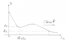
If you don't use resistor below 0.22ohm, then how are you going to satisfy Oliver's condition if you try to run beyond 120mA of idle current per stage?(120mA produce close to 26mV across 0.22ohm)
Simply as that: you don't. You may want to get the bias to point d2. The ridge between the Oliver point bias and class A corresponds to the gm doubling region (I guess you still do not have a grasp of this concept, it was mentioned several times in the last 24 hours). Physically, far up from the Oliver point, the transconductance peaks for the two halves are becoming broad enough so that their superposition is negligible. As a result, distortions are decreasing towards class A.
Because of their different conduction mechanism, power mosfets do not exhibit such a ridge. There is no optimal bias point for mosfets.
As a personal preference, I would definitely not get in the d2 bias point - IMO it's a poor trade between distortions and power dissipation. You either stay (at, or slightly over) the Oliver bias point, or you go deep class A and pay the full price. In d2 you will burn tons of idle power with very little benefit for the distortion performance. I think it was Mr. Curl that built in one of his commercial amps an externally switchable bias, one corresponding to the optimum Oliver bias, the other somewhere around d2.
Attachments
Hi Mr. Cordell
I need your help. Is 200mA per pair of EF, Re=0.12ohm dangerous? Should I do anything? I read you did say you won't use any Re less than 0.12, that's why I got the 0.12.
Thanks
Hi Alan,
Yes, I would say so. I think I said I would not go below 0.22 for RE. I don't recall saying 0.12 in the past, but I apologize if I did and misled you. Going below 0.22 is a point of diminishing returns. I like as big a class A region as possible, but one needs to consider the risk-benefit ratio. Also, the 26mV number is somewhat of an idealized number. The actual value for the optimum is often below that, as a result of ohmic emitter resistance and base resistance in the output device, and base stopper resistance.
Cheers,
Bob
Simply as that: you don't. You may want to get the bias to point d2. The ridge between the Oliver point bias and class A corresponds to the gm doubling region (I guess you still do not have a grasp of this concept, it was mentioned several times in the last 24 hours). Physically, far up from the Oliver point, the transconductance peaks for the two halves are becoming broad enough so that their superposition is negligible. As a result, distortions are decreasing towards class A.
Because of their different conduction mechanism, power mosfets do not exhibit such a ridge. There is no optimal bias point for mosfets.
As a personal preference, I would definitely not get in the d2 bias point - IMO it's a poor trade between distortions and power dissipation. You either stay (at, or slightly over) the Oliver bias point, or you go deep class A and pay the full price. In d2 you will burn tons of idle power with very little benefit for the distortion performance. I think it was Mr. Curl that built in one of his commercial amps an externally switchable bias, one corresponding to the optimum Oliver bias, the other somewhere around d2.
Thanks for the reply. do you have any link that explain more on this? I want to verify with you how I understand this. Attached is your graph with my notes.
1) At 200mA with 0.12ohm, I have 26mV across the Re. this is Oliver's optimization.
2) At 200mA but with 0.22ohm, I have 44mV across the Re. This moves into the GM doubling region. BUT because of the high bias, the kink is so smooth out that the distortion is not that bad. It's a little more as shown in your graph, but I do have a broad Class A region.
3) At point D2, the smooth out of the kink is so good that even though GM Doubling, it's still better than Oliver's optimization with 0.12.
My questions are:
1) How to determine D2? What mV across Re?
2) From your graph, sounds like distortion only depends on the bias current. Just want to check whether D2 be achieved keeping 200mA, but increasing Re to even higher than 0.22ohm? Or it is purely depends on the current.
Hi Alan,
Yes, I would say so. I think I said I would not go below 0.22 for RE. I don't recall saying 0.12 in the past, but I apologize if I did and misled you. Going below 0.22 is a point of diminishing returns. I like as big a class A region as possible, but one needs to consider the risk-benefit ratio. Also, the 26mV number is somewhat of an idealized number. The actual value for the optimum is often below that, as a result of ohmic emitter resistance and base resistance in the output device, and base stopper resistance.
Cheers,
Bob
Thanks Mr. Cordell
I am going to order the 0.22ohm then, if you look at Waly's graph and it makes sense that when I run at 200mA, it's high enough that even there is GM doubling, the kink is going to be a lot smoother, AND more importantly, I keep my big Class A region.
The last question, is 0.22 ohm safe enough?
- Home
- Amplifiers
- Solid State
- Bob Cordell's Power amplifier book