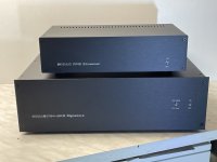
My parallel TDA1541A nos I2S dac is under construction. It is pure battery powered and direct supplying TDA chip. I used no regulator chip or capacitor on dac supply.
Attachments
Last edited:
My DAC at night 🙂
Incredible Grunf, it is essentially a power supply that can decode a digital signal!
Is that an AD1865?
Thanks, all the lights are Walt Jung shunt regulators 🙂 .
Not AD1865 but PMD100 + 8*PCM1702
Not AD1865 but PMD100 + 8*PCM1702
Some additional photos…My parallel TDA1541A nos I2S dac is under construction. It is pure battery powered and direct supplying TDA chip. I used no regulator chip or capacitor on dac supply.
My parallel TDA1541A nos I2S dac is under construction. It is pure battery powered and direct supplying TDA chip. I used no regulator chip or capacitor on dac supply.
Attachments
-
 WhatsApp Image 2024-08-08 at 16.34.15.jpeg287.7 KB · Views: 181
 -
 WhatsApp Image 2024-08-08 at 16.34.21(1).jpeg361.6 KB · Views: 185
 -
 WhatsApp Image 2024-08-08 at 16.34.21(2).jpeg420.5 KB · Views: 176
 -
 WhatsApp Image 2024-08-08 at 16.34.21(3).jpeg286.4 KB · Views: 162
 -
 WhatsApp Image 2024-08-08 at 16.34.21(4).jpeg322.7 KB · Views: 153
 -
 WhatsApp Image 2024-08-08 at 16.34.21(6).jpeg293.8 KB · Views: 155
 -
 WhatsApp Image 2024-08-08 at 16.34.21.jpeg350 KB · Views: 167
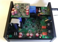
Here is my new diy ES9039Q2M DAC. Earlier I made a similar construction with Marcel's RTZ dac (see here). But since most of my music is in PCM format I decided to focus more on ES9039Q2M.


The DAC has a modular structure. There are 5 PCBs:

DAC has only USB input although I have a separate SPDIF/Optical board for ES9039Q2M. But the chassis is just too small to include that as well.
At the heart of the DAC is my STM32H7 based USB-I2S board which also acts as a controller for UI/encoder and DAC (via I2C/GPIO). All DAC signals (I2S/I2C/GPIO) are isolated. Clocks are NZ2520SDAs but external clocks can also be used. On the bottom side is a battery for backup RAM (and RTC). The display on this DAC is ST7735-based but also a display with touch screen could be used as 2 SPIs are available at the 20-pin connector. The SW is running on FreeRTOS. UI and DAC controller task have lower priority while USB-I2S has highest priority. Tasks are decoupled with message queues to minimize interaction. The USBI2S board supports up to 768k/32 PCM or DSD512/DOP256 (no ASIO driver so native DSD only on Linux). Even 8/16 channel TDM is possible although not used in this DAC.


Headphone amp is an Omicron clone. Main difference to original are smaller size and onboard headphone connector. Crossfeed is switchable from UI.
PSU is a "SilentSwitcher" supporting USB PD.
Chassis is a Hammond 1455N1601 (160x103x53mm).
Here are some pictures of the DAC UI. ES9039Q2M has loads of configuration options but I have incorporated only those I've found useful.


Performance of the DAC is top-notch. Here is 0dBFS through Cosmos APU to AK5394. No THD compensation used.

The DAC has a modular structure. There are 5 PCBs:
- DAC
- USB-I2S
- Controller (UI & encoder)
- Headphone amp
- PSU
DAC has only USB input although I have a separate SPDIF/Optical board for ES9039Q2M. But the chassis is just too small to include that as well.
At the heart of the DAC is my STM32H7 based USB-I2S board which also acts as a controller for UI/encoder and DAC (via I2C/GPIO). All DAC signals (I2S/I2C/GPIO) are isolated. Clocks are NZ2520SDAs but external clocks can also be used. On the bottom side is a battery for backup RAM (and RTC). The display on this DAC is ST7735-based but also a display with touch screen could be used as 2 SPIs are available at the 20-pin connector. The SW is running on FreeRTOS. UI and DAC controller task have lower priority while USB-I2S has highest priority. Tasks are decoupled with message queues to minimize interaction. The USBI2S board supports up to 768k/32 PCM or DSD512/DOP256 (no ASIO driver so native DSD only on Linux). Even 8/16 channel TDM is possible although not used in this DAC.
Headphone amp is an Omicron clone. Main difference to original are smaller size and onboard headphone connector. Crossfeed is switchable from UI.
PSU is a "SilentSwitcher" supporting USB PD.
Chassis is a Hammond 1455N1601 (160x103x53mm).
Here are some pictures of the DAC UI. ES9039Q2M has loads of configuration options but I have incorporated only those I've found useful.
Performance of the DAC is top-notch. Here is 0dBFS through Cosmos APU to AK5394. No THD compensation used.
Grunf,Thanks, all the lights are Walt Jung shunt regulators 🙂 .
Not AD1865 but PMD100 + 8*PCM1702
are regulators your Walt Jung / Didden super regulator (available at diyaudio) execution or kind of modded Walt Jung regulator
Almost 25 years ago, with the good old PCM63 ... 😊


All regulators are modified shunt regulators from Walt Jung. A total of eight different ones with voltages of 2x3,3V, 2x5V, +/-5V and +/-14V.Grunf,
are regulators your Walt Jung / Didden super regulator (available at diyaudio) execution or kind of modded Walt Jung regulator
I don't use serial regulators(Walt Jung / Didden super regulator) in the DAC.
Attachments
All regulators are modified shunt regulators from Walt Jung. A total of eight different ones with voltages of 2x3,3V, 2x5V, +/-5V and +/-14V.
That would make things sing nicely. Well done.
@bohrok2610 ,
Should be quite imune with that small form factor and the external PS. Number max of layers on a single pcb, seems good two layers classic as I do not see much vias ?!
What are please the smallest casing case you usefor caps/resistors ? You work with a hote plate or owen ?
Do you use an op amp for that dac chip or has it its own V output ?
That compactness is very inspiring, congrats.
All PCBs except controller board have 4-layers. Many of the vias are on pads so not visible. I haven't found via fencing (or similar) necessary.Number max of layers on a single pcb, seems good two layers classic as I do not see much vias ?!
Smallest size is 0603 for caps and resistors. I use a reflow oven.What are please the smallest casing case you usefor caps/resistors ? You work with a hote plate or owen ?
I/V op amp is a composite.Do you use an op amp for that dac chip or has it its own V output ?
Honestly yes. Thanks. The regulators really take the whole DAC to a higher level regardless of the fact that the whole DAC is old school. ( the regulators themselves use 4pcs ADA4897 and 4pcs ADA4625-1 with some 24pcs various depletion mosfets)That would make things sing nicely. Well done.
Let me show some photo of the latest DAC.
Based AK4491+AK4499, with ALL inputs galvanicaly isolated, XMOS USB, Sync/ASync operation for all inputs (except USB), Master/Slave MCLK at I2S input.
MDAC Analogue Volume Control, separate headphone amplifier, IPS display, touch sensor control, IR remote control.
No switching regulators or power supplies, except DC-DC for I2S isolated input.
Totally 5 PCBs: Main PCB, I2S/XLR PCB, DAC PCB and Front Panel PCB.
Alex.
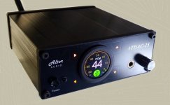
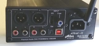
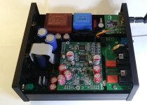


Sorry, + 5th PCB with Bluetooth.Totally 5 PCBs:
P.S. BT power and HDMI-I2S DC-DC are off when not used, to decrease the noise and power consumption.
All firmware (XMOS and STM32) are user upgradable.
Totally - 20 voltage regulators used.
- Home
- Source & Line
- Digital Line Level
- DAC gallery
