Not anymore. The linear PSU completely eliminated the turn-off thump.
I think it should be easy to completely linearise a power-wall supply.
My build is coming along slowly, but I can now report that half the amp works haha. I switched it on in my unheated workshop, connected to an old Squeezebox Classic and a pair of old test speakers.
One channel had glorious sound, the other was silent. As the temperature outside was dropping fast and my help (who is 24, not interested in electronics or audio but a great help with this build nonetheless) really needed to go home, I decided to call it a day. I hope to find out what is wrong with the other channel in a few days when I can organise someone to do the lifting and other stuff for me. It could simply be the speaker cables.
The only bit to do after that is recheck the voltage, connect the LED and tidy up the wiring. And of course enjoy it!
Last edited:
^ That might be interesting. What are you suggesting?
To start off, a simple follower can be used.
I think the K-multiplier (by keantoken) is great, there is a version for high current, and drop-out is low. A simple capacitance multiplier just a Rcb and a cap Cb-earth already works.
A Mosfet has too high a drop voltage, but I remedied that myself with a voltage doubler (but then I had a transformer input). So that is what I use. I found a mosfet with an active circuit that clamps at some high current. [Like an active fuse, great to have with SITs]
Elsewhere I currently have a CCS based on a FET, and a resistor to set the "bias" of an output device//a capacitance, a NPN-transistor, but I use that for a preamp (JFET buffer, that is).
So my most advanced idea:

A version with a LoVoltech (LU1014D-look alike) could be interesting. Low drop. And just have a .25 ohms at the source, it limits the turn-on; even with [for example] a CL-50 NTC Inrush Current Limiter, on resistance is 0,2 and once operational the FET is always on. With a resistor of Rg-out 2 k & then a 2 uF Cgate-earth for the ramp-up.
I need some ZEN feedback for this

Will it work? Is the Vds max an operational problem?
I don't have the model, sorry; I ordered but still to receive.
If you mean a simple cap multiplier like Juma’s easy peasy cap Mx but with a LD1014D/LU1014D to reduce dropout? You have problem that JFET is depletion device and is only good for 20v.
You still need some dropout to provide the regulation. I have found it’s hard to get less than 3v if you really want to flatten the ripple. The CFP based BJT cap Mx I use is adjustable and I find that 3v seems to be the ideal drop for low ripple output use.
You still need some dropout to provide the regulation. I have found it’s hard to get less than 3v if you really want to flatten the ripple. The CFP based BJT cap Mx I use is adjustable and I find that 3v seems to be the ideal drop for low ripple output use.
To reduce ripple while maintaining dropout=3V, you can get spectacularly lower ripple than a single CFP, simply by cascading three single BJT capmuls in series. The key idea is to use Sanken 2SC4024 NPNs, DigiKey sells them but Mouser does not. Mouser also doesn't sell Edcor transformers but that never stopped DIYers from using Edcors.
BTW for output current less than about 2 amperes, the Sanken 2SC3852 is even better.
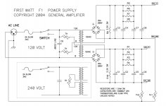
The above applies to single rail power supplies such as the Sony DIY VFET amp (the subject of this Forum thread).
_
BTW for output current less than about 2 amperes, the Sanken 2SC3852 is even better.
The above applies to single rail power supplies such as the Sony DIY VFET amp (the subject of this Forum thread).
_
Attachments
The SLB boards that I built drop about 2 Volts in the rectification section, and about 3 Volts across the CFP. Output ripple is about 2mV, as reported by my DMM. I haven't put a scope on it yet. There is a very faint 120 Hz hum that is only detectable when my ear is right next to the speaker. This suggests some harmonics of 60 and 120 Hz are present as well. I expect this would disappear completely if I added some bulk capacitance to the power rails inside the amp chassis.
I have considered trying a simple shunt regulator before the CFP. Something like a TL431 controlling a suitable PNP transistor. The intent would be mainly to stabilize the output voltage a little more. Though the ripple is very low, the voltage does fluctuate slightly with changes in the mains voltage. My refrigerator is the main culprit.
Those Sanken devices are pretty interesting. Darlington levels of hfe without the large Vbe.
In a version of Le Monstre (8 watt out of a 25 kg amplifier chassis) I used a shunt like that. TL431 and a darlington, a TIP145 if I recollect well. Even with 100 mA it got rid of the hum.
THat brings me to think, as I am now building a choked-SIT, to do that again. So thanks for the inspiration.
You know, 25 Volts at 2-3 amp per side is not a trifle. Even for a TIP147 as pass element.
So that would be usefull also for the VFET users.
I had 0,5 ohm in front and after the shunt. The 8 watt Hirage needed 1.2 Amp per side at +/-13.2 volt (because of using "10V super caps" that can go a little higher than 10V - that is, without AC component)
It worked very well. THat brings me to think, as I am now building a choked-SIT, to do that again. So thanks for the inspiration.
You know, 25 Volts at 2-3 amp per side is not a trifle.
Even for a TIP147 as pass element.I have 7 uH 0,1 ohm inductor directly after the bridge that eliminates all switching hazards, but after that inductor, even with 12.000 uF there is still 150 mV RMS hum.
Need to have that low low low. Ben Mah's choke-load will give away any noise to the output, for free!
Need to have that low low low. Ben Mah's choke-load will give away any noise to the output, for free!
So that would be usefull also for the VFET users.
The SLB boards that I built drop about 2 Volts in the rectification section, and about 3 Volts across the CFP
The rectification is an LT4320 active bridge and low RDson MOSFETs so very low voltage drop. In fact, I think you gain 1.2v that normally would have been lost from Si diodes in a traditional full wave bridge. The 2v drop is more likely the drop across the R of the CRC. What is the R value of your CRC? 2mV ripple is about right. I measured about 1.3mV rms with a scope.
@Mark Johnson: a triple cascaded BJT is also interesting. You would be dropping at least 1.8v then plus some extra headroom for regulation. Although on my amps, when ripple output of cap multiplier is circa 1mV, no noise is audible at the speaker so do we need more ripple reduction?
Yeah, the 2V (plus) drop for rectification includes the drop across the R of the CRC, and a little more since the transformers are overachieving even under load. The R value is 0.2 Ohms total, so about 0.34V drop across that when loaded by the fully warmed up amplifier. The input to the CFP sees about 39 Volts, depending on AC line voltage.
so do we need more ripple reduction? [Isn't sub-1mV good enough?]
Then eliminate the third NPN cascaded stage and reduce the in-to-out DC drop. The benefit of 2 stages is -40dB/decade attenuation compared to -20dB/decade in a single stage. 3 stages gives -60dB/decade of course.
I’m bit confused by what seems to be a lot of complex proposals regarding a linear power supply for this VFET amp.
I don’t personally feel compelled at this point to try one and am very happy with the way the amp sounds and functions.
I understand others may just have their own reasons or perhaps the thumping on turnoff is reason enough for them.
In the past I had thought of trying linear supplies for my ACA monoblocks.
That was in part to see if there would be a sonic improvement, but also because I thought the tangle of the dual SMPS brick supplies was bothersome and I would have liked a PS case with a switch on the front that the ACAs could stack on top of.
That being said, I had always assumed since these designs function on SMPS bricks, or a mono rail power supply, that I would just use the supply designed for the F1 as I did when I built my F2J monoblocks.
Am I completely wrong about something here?
My F2J amps are dead silent with this design and have no turn on or off thumps.
Attachments
The show stopper song from the musical "Plain And Fancy" (1955) seems to offer appropriate, and beneficial, advice here.
Follow Your Heart
Follow Your Heart
I have viewed this as an exercise in revealing the full potential of the amplifier. The SMPS that is part of the kit does a good job and will make some (or most) amp builders very happy. It is a cost effective solution. It does not let the amp perform at its very best. The only way to find this out is to build an alternative PSU and listen carefully to the results.
The discussion of alternate linear PSU designs is a way of exploring different ways of letting this VFET amp sound its very best.
The discussion of alternate linear PSU designs is a way of exploring different ways of letting this VFET amp sound its very best.
.................
My F2J amps are dead silent with this design and have no turn on or off thumps.
The F2J was designed to have no turn-on thump:
DIY F2 clone
If you send music to your F2J and then turn on your F2J, you will notice that a few seconds will elapse before you hear any music from your speakers.
")
Alas, I had hoped my one channel vfet would turn into a stereo vfet today, but it has not. The working channel sounds really nice, even on crappy speakers, but I have come to prefer stereo if at all possible
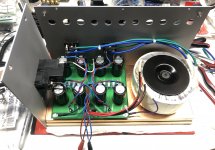
I rechecked the adjustable voltage on both OS boards (20V as expected) and concluded both OS boards have power (so power wiring is OK). This was also obvious when both heatsinks warmed up nicely.
I checked that I had power on both FE boards (yes), and continuity tests showed the input RCA's were correctectly connected to the FE boards and the FE boards were correctly connected to the OS boards. No continuity between the RCA wires themselves, so no accidental short.
I then swapped L and R inputs (in case the problem was in the source or interconnects; no change) as well as L and R outputs (in case the problem was in the speakers or speaker cables; no change) but the problem has remained to be confined to the left channel of the amp.
So, I think the problem is either in the left FE board or the left OS board.
Luckily I used terminal blocks to connect all the wiring to my FE boards, so did not have to desolder the wiring. I have now taken both FE boards out of the case, and checked see if I made any stupid mistakes like orientation of the fets (fine). I also checked the resistance of the primary and secondary windings of the Edcors of both FE boards (on the rear of the pcb, where they are soldered on the boards) and they are similar. So, not sure what is wrong. I probably made a mistake somewhere, just haven't found it yet
I think my next step is do tests on a single channel at a time to figure out where the problem is. I will try different combinations (FE1 + OS1, FE2 + OS1, FE1 + OS2 and finally FE2 + OS2) and hope to pinpoint the problem. Once I know which board is causing the problem, I hope to figure out what I did wrong. Any suggestions about what to look out for are welcome.
Note: I do have 2 different FE boards (one final and 1 prototype) and the traces on the left side of the board are quite different. I assume no faulty proto-prototype boards were shipped lol.
- Home
- Amplifiers
- Pass Labs
- DIY Sony VFET Builders thread