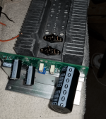
VFET and MOSFET are secured to the heat sink (4650) for one channel. I guess I just have to connect the wires in the right order to the input board and add V+ to test the heat sink viability. Can V+ be ramped up slowly, or should it be turned on at full V? What is the proper current/amp setting for a variable power supply? The transistors with the flexible junction wafers are on the underside of the heat sink, the attachment apparatus is on top. Attachment apparatus is what is showing (S, D, G).
I'll wait until next week when I get back to try out the V+, do a check over first and then see if the thing blows up.
I'll wait until next week when I get back to try out the V+, do a check over first and then see if the thing blows up.
Attachments
Last edited:
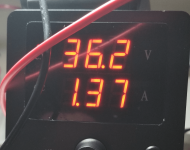
OK, I was curious so I hooked it up to V+. It didn't blow up, so I assume it is OK. The variable power source read around 36.3 v and 1.37 amps or so with no adjustment. I imagine adjustment will make the amps a little lower.
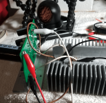
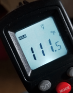
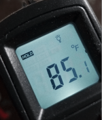
After about 40 min., the 'hot' side of the heat sink seemed to stabilize about 130 F. The 'cold' side of the heat sink seemed to stabilize around 95 F. I could touch the heat sink for several seconds most of the time at greater than five seconds.
I will have to check it again later when I get back next week.
Attachments
So, raw out of the chute, it is 'overclocked' by about 5 watts dissipation or so over Ben Mah's calculations. I surmise adjusting the varistor or something will drop it down to the 44 or 45 watts or so instead of the 49.6 to run a bit cooler, or at least I hope so.
I am going to read NP's OS2 .pdf again while away from home. However, it looks promising that I got the components in there correctly.
I am going to read NP's OS2 .pdf again while away from home. However, it looks promising that I got the components in there correctly.
130 F is about 54.5 C so it's getting up there in heat.
1.37A is a bit higher than the specified 1.2V/0.94R=1.28A through R1+R2, so that is the reason for your higher power dissipation.
However R1+R2 (0.94R total) is in the path of the 1.37A so they dissipate 1.37A x 1.37A x 0.94R= 1.8W. Therefore the the heat sink dissipates 1.37Ax36.3V - 1.8W=47.9W.
You can lower the power dissipation by reducing the CCS current. Increase R6 (N VFET) or R7 (P VFET) will decrease the current.
Thank you again. I don't know if I mentioned I am doing the N channel boards with 2SK60's. What value R6 would you recommend? What exactly does the variable resistor (P1 50K)do exactly? It may be around in the literature, but I can't find the specific function of that item, I would assume it adjusts something in there.
My readings were taken from the variable voltage supply readout, so I don't know how accurate they are. I presume I should be taking readings from the board as well with a proper volt meter.
"Potentiometer P1 is used to set the DC output voltage, which is +16 VDC measured on the case of the IRFP250 transistor."
I guess I will have to ponder that part from NP's document until I get it.
To decrease the current I suggest increasing R6 by 1K or more. You can temporarily series connect some resistors. In my own diy amps I have a trimmer pot instead of a set resistor so I can easily adjust the current. So increase R6, measure the current, adjust some more if necessary.
However if you have not adjusted P1 for 16VDC at the IRFP250 case (drain), do that first and then check the current. To check the current, measure the voltage across R1 and use Ohm's Law to calculate the current: I = V/R.
P1 adjusts the VFET bias voltage (Vgs) which controls the drain to source DC resistance of the VFET. This resistance combined with the drain current set the voltage drop across the VFET. In this circuit, the net effect of adjusting P1 is that it adjusts the voltage at the 2SK60 source. Since the case of the mosfet (drain), is connected directly to the 2SK60 source, it is used to measure the voltage at the 2SK60 source. The mosfet case is easily accessed whereas the VFET source pin is not easily accessed for voltage measurement.
My concepts are starting to gel on the circuit diagram. Measure and adjust the 16v at the MOSFET pin/case with P1. Also, the test rig for the heat sink is sitting on a towel, whereas the heat sink when placed in the chassis is bolted also to the main chassis and has an air space underneath. I'll elevate the heat sink a bit off the towel to get an air space. I don't imagine having the heat sink on an insulator helps. Adjusting the VFET Vgs bias will likely help, and plan B would be adding incremental 1k resistance at R6.
Does dropping the bias current on this unit just drop the power output, or are there other disadvantages? How low could the power draw go if the bias current is dropped and still have a viable amp? What if the target was 6w nominal instead of 10w nominal?
I feel kind of lonely here, or did NP saturate the Greedy Boyz with his generous giveaway?
I feel kind of lonely here, or did NP saturate the Greedy Boyz with his generous giveaway?
Plenty of disadvantages - higher distortion is one of them, reduced ability (strain) to drive difficult loads, which also brings the distortion up, is another one.Does dropping the bias current on this unit just drop the power output, or are there other disadvantages? How low could the power draw go if the bias current is dropped and still have a viable amp? What if the target was 6w nominal instead of 10w nominal?
I feel kind of lonely here, or did NP saturate the Greedy Boyz with his generous giveaway?
If you want to convert it to a head amp it will work but I would still not recommend it.
Linearity will be very much compromised and then what's the point of having such amp?
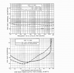
Just for fun, the measurements of the Sony TA4650 amp from the day. The article deemed it a 60w/ch amp in spite of 30w/ch rating:
My initial impulse at this point is to install the NP N channel amp sections in the 4650 chassis and use the working volume controlled internal preamp section to feed it. I have bulwark cards, but I think I would do that later. Internal preamp of 4650 is (I think) a simple (cascode ??) FET per channel with another FET cascode added if the tone controls are engaged. Output impedance is listed in manual as 3Kohm, which seems a bit high? Maybe an internal Korg board later or bulwark FE (if workable)? Managing the room inside is the challenge, but two SMPS fit so far with room to spare.
I will continue to bench test the single heat sink for two channels, but I suspect I will eventually use two heat sinks which will fit in the chassis when used vertically instead of horizontally. Question is if the single heat sink can dissipate the 90 watts of heat, which is just a maybe. The original heat sinks were designed with the transistors downward, with a heat chimney effect pulling air from the bottom space into and over the heat sinks. Specs on the TAN 8550 (which used these heat sinks) seem to indicate that the idling wattage was over 100 watts/ch per heat sink, so that would be within a 90 watt spec, but who knows what the variables are.
Attachments
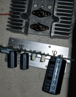
OK, it appears so far I have two working N channel cards assembled that bias to the 16v on the drain pin of the MOSFET on my bench rig. I pulled some major dumass boners that are a bit embarrassing to recite, but I will if somebody is interested. Fortunately, it did not result in the loss of any transistors or VFET (again, first amplifier build. I built Korg B preamp successfully a while ago, my first full DIY endeavor).
Having the MOSFET/VFET lashed to one end of the Sony TA 4650 heat sink, things on that end seem to stabilize temperature wise at about 120 F on the heat sink, maybe ten degrees hotter on the transistor cradle. I lifted the heat sink off of the towel so that it was surrounded by air and that seemed to reduce temp overall by about 10 F.
I can hold my finger on the adjacent heat sink for five to ten seconds. At the other end of the heat sink, it stabilizes at about 90-95 F.
I guess my next will be to continue testing heat sink on bench to see if I use two heat sinks or can get away with one, and hook up a source and speaker to a card to see what kind of noise it makes. If that goes well for two cards, the next will be how to decide to get the rig into the 4650 chassis. My present thought is to use the built in 4650 preamp to drive the amp units and decide on putting in the Bulwark cards later. I have no idea what the gain is of the built in preamp and it has a 3K ohm impedance output according to the literature. Maybe that could be a problem in impedance matching. However, the preamp section has lots of tone controls and inputs and is routed through its own output, with the power amp section accessed through its own input, easy to unplug.
Last edited:
- Home
- Amplifiers
- Pass Labs
- DIY Sony VFETs OS2 Official thread