Hi OS, do you have the latest and greatest LTSpice?
Can you convey the news on this? Development has not totally halted after the head dev left?
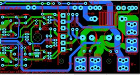
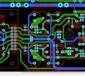
I like this new EMC layout. Low loop areas.
Looking further, the feedback signal and ground traces are very far apart. The low loop area in the output section will mitigate this issue but the feedback loop area is pretty large. Furthermore the speaker return shares a conductor with the PSU cap return currents. Unless G1 is meant to be speaker return. How about putting the speaker return terminal under the output terminal, running a fat trace to G1, and then sampling the feedback ground from a point along that trace next to G1? This way nothing shares a conductor with PSU currents.
To reduce the feedback loop area, why not run the feedback trace parallel to to the frontend ground trace and then use a jumper next to the output inductor to get to the output point? I think the jumper is definitely worth it in this case.
Thinner traces would help dodge between pins and reduce the loop area. Thinner traces have higher self-inductance but the losses you take from large loop areas are disproportionate in comparison.
Last edited:
Hi Keantoken,I like this new EMC layout. Low loop areas.
Looking further, the feedback signal and ground traces are very far apart. The low loop area in the output section will mitigate this issue but the feedback loop area is pretty large. Furthermore the speaker return shares a conductor with the PSU cap return currents. Unless G1 is meant to be speaker return. How about putting the speaker return terminal under the output terminal, running a fat trace to G1, and then sampling the feedback ground from a point along that trace next to G1? This way nothing shares a conductor with PSU currents.
To reduce the feedback loop area, why not run the feedback trace parallel to to the frontend ground trace and then use a jumper next to the output inductor to get to the output point? I think the jumper is definitely worth it in this case.
Thinner traces would help dodge between pins and reduce the loop area. Thinner traces have higher self-inductance but the losses you take from large loop areas are disproportionate in comparison.
There is alot of very useful information in that post. To make it clear, is it possible to add / sketch the speaker return and other traces you mention to the circuit image as an overlay.
A picture tells a 1000 words as you know.
")
I like this new EMC layout. Low loop areas.
Looking further, the feedback signal and ground traces are very far apart. The low loop area in the output section will mitigate this issue but the feedback loop area is pretty large. Furthermore the speaker return shares a conductor with the PSU cap return currents. Unless G1 is meant to be speaker return. How about putting the speaker return terminal under the output terminal, running a fat trace to G1, and then sampling the feedback ground from a point along that trace next to G1? This way nothing shares a conductor with PSU currents.
To reduce the feedback loop area, why not run the feedback trace parallel to to the frontend ground trace and then use a jumper next to the output inductor to get to the output point? I think the jumper is definitely worth it in this case.
Thinner traces would help dodge between pins and reduce the loop area. Thinner traces have higher self-inductance but the losses you take from large loop areas are disproportionate in comparison.
Just the guy I was waiting for !!
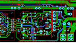
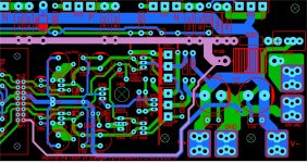
1. - (below 1) is this what you meant for the GND return of the speaker ??
2. - (below 2) no jumper. NFB follows the G1 - G2 trace .
3. I have servo "blues" . Do you think a servo is even worth it ?
A. Complexity .... Vregs , IC , etc. Many builders come over from the tube
and Pass world.
B. Subjective discrimination - Just don't like chips. Bet they have lots of chips , hypocrites.
C. Performance hits - Even with MORE complexity , 2'nd order filters ...LF
THD suffers.
I have the chipless version (below 3) , all ready to go and tested.
Just the cap , diode reference (and trimmer) to offset NFB. A manual servo.
Without the servo , this design is sub - PPM throughout most of the audio band.
Any comments ?
OS
Attachments
Last edited:
1: That is pretty much what I was envisioning, although I would tap off the speaker ground to star ground trace instead of going to the middle of the star ground. This is one situation where I err slightly toward bus grounding, and this logic has served me well.
2: Pretty close to what I imagined, but I was thinking the feedback traces would go under the PSU connectors and around the speaker ground connector. That way the feedback traces can share less loop area with the capacitors, even though they end up a bit longer this way.
3: To me the main reason I have considered servos was to eliminate the feedback DC blocking capacitor. If it still needs that cap I have no idea what it is for. If the point of using a servo is merely to get <1mV offset, then it really has no purpose subjectively or for performance.
4: The offset trimmer has little or no wiper current... This can cause problems with the wiper not being able to clear oxidation. Often overlooked, even in test equipment circles.
5: We can continue searching for other currents that share a conductor with the feedback ground, and the most notable are the cap multiplier input capacitors. You are actually more likely to get distortion from the return currents of these capacitors than you are from the minor loss of PSRR if you just removed them. That is to say, in the current layout they don't improve PSRR, they actually worsen it, because they share a conductor with feedback ground. This is real experience talking here... My suggestion, if you don't want to run a separate ground, just remove them and their 100nF bypass. The cap multiplier collectors easily deal with the extra inductance, unlike chip regulators. They should be stable with the 100uF output capacitors, and it should be easy to confirm this in the bench test. If not then the smallest, lossyest lytic capacitor at the collector should suffice (I've seen 0.22uF electrolytic capacitors).
Beyond this the VAS carries OPS drive currents which contain harmonics which may or may not be large enough to contribute to THD through the shared feedback ground conductor. I am uncertain the strength of the effect. But it should be possible to simulate it with an inductor in the feedback ground path shared by the frontend PSU capacitors.
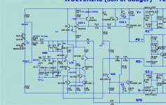
Looking at the schematic, check what happens to the LTP cascode voltage on positive clipping. When Q3 saturates, Q5 will conduct it's base current and pull down the cascode voltage toward the negative rail, possibly exceeding the voltage rating of the LTP transistors. Just shooting from the hip here.
1. - . I know the PS cap return currents
mostly cancel out at the center of the star.
So what you mean is tap G1 right from the center of the speaker ground.
There, the +/- from the outputs also cancels ?
2. - Is there anything really wrong with that FB route ? With P/N alternating
outputs , would not the whole output trace be the same ? (between any P/N output Re's
This was discussed
earlier. I listened , and went right to the OP coil.
3. - So you don't like servo's ? Neither does Elliot (ESP).
4.- Trimmer - Bourns 3006 series is hermetically sealed. Oxidation ??
5 - Cap- mult. input caps ? You mean C103/4/7/8 ? They decouple the
driver pre-driver rails , are needed for the EF3. I could give them a separate
pair of returns ... but they are essential to the design.
I did it , (below) C101/2/5/6 return separate from C103/4/7/8.
OS
Attachments
Looking at the schematic, check what happens to the LTP cascode voltage on positive clipping. When Q3 saturates, Q5 will conduct it's base current and pull down the cascode voltage toward the negative rail, possibly exceeding the voltage rating of the LTP transistors. Just shooting from the hip here.
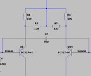
50Vce at clip - Q1/2. So , BC547/8, BC557/8 out of the question.
BC546/556 could/should be OK.
Good observation.
OS
1: Tap off feedback ground somewhere along the trace that connects G1 to speaker ground. More toward G1 because then feedback ground shares a conductor with speaker return, which does have an effect. You just want to be slightly away from the star ground mixing point. Right at the via is already far enough from the mixing point, but speaker ground can't be routed to the via, so the next option is to tap off the trace that connects speaker ground to G1.
2: The half sines follow the same path through the power traces and thus combine into a clean wave in the magnetic field, until they reach under the output inductor where they split again. This is the main radiated hazard to the feedback signal which runs right next to it. Run the feedback signal and ground pair right next to each other right up to the output and speaker ground terminals and they will be immune to it. The speaker ground terminal and feedback ground should be close to the star ground mixing point without ending up on opposite sides of it.
3: I like servos only for the purpose of eliminating the feedback DC blocking cap, I don't see any other justification. Honestly with a cascoded LTP and that current mirror, do you even need the feedback cap or servo anymore? You have eliminated most offset mechanisms, I suppose you still have the Hfe tempco of Q13.
4: Yeah, that's what they all say. In the discussion I learned about this, some sealed Bourns trimmers of unexpectedly poor quality were discussed. Personally I gladly take the hermetic sealing as an improvement to reliability but I don't assume that I can forget about it. There is a reason that newer test equipment is using DACs and digital resistors rather than resorting to trimmers.
5: Good point, running a separate ground is the logical thing to do then. Or maybe just give signal it's own ground run entirely and leave G2 ground only for power.
With the inverse square law, if you reduce emissions by 4x then you only have to halve your distance before the noise level is the same again. So just because the rail currents run next to each other is not a good reason the feedback pair can be run right next to them.
I must admit that is a very tempting suggestion. The feedback pair would run next to the output trace, but that current loop is 90 degrees to a top/bottom routed feedback pair. I think it is probably a good option if it could be done, but routing along the bottom still keeps the feedback pair further away from the main radiating area overall.
Edit: the problem was that the feedback signal and ground traces were on opposite sides of the drivers and power input section. This creates a loop that is in the same plane as the speaker current loop and the power input capacitor loop. If you run feedback and feedback ground as a top/bottom pair this is largely solved. The issue is how to route it so that when we have to separate the traces again, the loop that creates will also not be susceptible to other current loops.
Last edited:
With the feedback trace running along the output rail the currents will be flowing in opposite directions in both traces at all times. Will this not cancel each others noise emissions?
This is what I am hoping for in this reiteration (below).
Notice where the (pink) NFB trace reaches the "chokepoint" between C115 and
R113. I added the cancelling second side opposing V- right up to C115.
At the "chokepoint" NFB is between V+ and - (closer to V- driver rail).
Would it negate ??
Come to think of it .... if someone wants to get really anal , one could run a shielded
cable right to the IPS interface.
OS
Attachments
Another question if I may.
What are the drawbacks, negative side effects of using a potentiometer in the ltp emitters to zero the output offset ?
I have read on the forum people dislike this, just wondering why
edit. or is it the wiper oxidising as explained in a post above, here the wiper should have 800uA to 1mA, depending on ltp bias
Attachments
Last edited:
Yes, I actually did do the shielded feedback run once. Luckily I don't seem to have need of that trick anymore.
The leg of V- extending to C115 will do nothing because the currents running through it are not the counterpart to the trace below it. It is currents we are guiding, and currents only flow from source to destination through the easiest path.
You can visualize the input power current loop like this. The output stage rectifies the output current into a half sine pulled from the positive rails, and another half sine drained into the negative rails. Below the output inductor, the half sines split. The positive half sine flows from the positive terminal up and to the right in a clockwise fashion. Then the negative half sine flows to the right and down, completing another 1/4 turn of the clock. The currents complete the lower half of the clock in the power input wires where they come together in a twist. So the resulting radiated waveform is a rectified sine wave current flowing in a clockwise circle in the general area of the capacitors.
The negative half sine travels under the inductor and to the right, ignoring the branch to C115 completely. In order for the current to take this branch, the V- terminal would need to be at the end of it.
What are the drawbacks, negative side effects of using a potentiometer in the ltp emitters to zero the output offset ?
The wiper will be fine because there is enough current flowing through it to clear any oxidation. The condition of very low wiper current is a special case where the trimmer becomes susceptible to going open and I'm not sure this is affected much by the seal.
Some trimmer compositions would oxidize over time affecting the trimmer resistance or usually just making the wiper unconductive through large areas of the adjustment. I have trimmers like this in my tired old FG504 signal generator - one of the ones I had trouble with is a sealed trimmer. But the sealed trimmers are still more reliable overall.
Basically the trimmer does what it says on the tin in this case. It's not any worse than normal resistors in the same position, except if something goes wrong with it, which is frankly pretty unlikely. Even if the wiper disconnects, the only effect it has will be to worsen offset.
Some of the dislike of trimmers is just an OCD-like nonspecific disgust that gets the better of some people. Such sentiments usually dissolve when one has the opportunity to survey a range of real examples and see what actually fails and how often.
On that note, I thought OS was doing a lot of repairs at one time, so he probably has more experience with failed trimmers than I do. Maybe I should be the one listening...
Another question if I may.
What are the drawbacks, negative side effects of using a potentiometer in the ltp emitters to zero the output offset ?
I have read on the forum people dislike this, just wondering why
edit. or is it the wiper oxidising as explained in a post above, here the wiper should have 800uA to 1mA, depending on ltp bias
1.Possibly safety . if the wiper disconnects poof ! NFB based offset ,
if the trimmer fails , still have the DC cap bias as backup.
2. unbalanced LTP local FB (different Re's).
I did the LTP trimmer on the Badger
.... this is not the Badger.OS
The trimmer can appear to unbalance the LTP degeneration, but this is an illusion. The LTP tail does not conduct any audio current so even if you turned the trimmer all the way in one direction you would only succeed in changing the voltage swing at the CCS. You would change the amount of degeneration though by shorting one of the fixed resistors with the wiper.
All audio current flows from one emitter to the other in the LTP, where exactly the CCS taps off in the midst of that resistance does not matter. Okay, if it is not a perfect CCS than your CMRR suffers due to unbalanced degeneration.
I just proved myself wrong, that's how I know I need to stop talking...
- Home
- Amplifiers
- Solid State
- DIYA store "Wolverine" (Son of Badger) .... suggestions ??