Hi, does anyone know how I can change the filtering curve steepness (called filtering modes?) on the ES9038Q2M ? (Iancanada's dual mono board for RPi).

I would use it via Volumio but without any screen or buttons, no addons at all. Is the filtering set in some kind of config file or so in this case ?
I would use it via Volumio but without any screen or buttons, no addons at all. Is the filtering set in some kind of config file or so in this case ?
Vortex, The chip has several selectable filters or custom coefficients can be entered. All filter programming is over I2C bus, as is all other register programming.
It takes an MCU or CPU of some kind to act as I2C bus master and control the dac chip internal registers.
We could help show you how to do that with an Arduino or possibly with an RPi, otherwise you may be out of luck.
It takes an MCU or CPU of some kind to act as I2C bus master and control the dac chip internal registers.
We could help show you how to do that with an Arduino or possibly with an RPi, otherwise you may be out of luck.
Hmm. Thanks. I'm pretty sure the default setting would sound great too at first sight - maybe also on the long run - but it would be interesting to experinent with this.
Would a IANCANADA ESS Controller kit help ? (I assume yes, just making sure). However, I wouldn't even need the display at all, nor the whole stuff, just a way to switch between filtering modes with a press of a button or via software.
Arduino, hmm. My next big deep-dive on my bucket list. I might need one anyways for power ON/OFF switching (from fully ON to standby, where only this Arduino is powered via the main switch and it's controlling all other components' power via a relay).
Would a IANCANADA ESS Controller kit help ?
What it can do is described manual which can be found at: DocumentDownload/ESScontroller at master * iancanada/DocumentDownload * GitHub

Something I have been meaning to mention for the last few days: Just had the bad experience of blowing up the I2C pins on a couple of 3.3v Arduino Pro Trinket boards. Why? The Schottky diodes I use for I2C pin input protection. The diodes are supposed to clamp the I2C pins from being able to rise too far above the Arduino's Vdd pin (which could happen when using external I2C pullups that get powered on while the Arduino itself is still powered off.
As it happened I ran out of the usual diodes for that, and substituted some Schottkys not too different from the old ones (so I thought). However with the alternate diodes, seems that some sort of transient occurs at Arduino power-on that blows the pins. Switched back to the regular diodes which have a bit higher forward voltage but less reverse leakage (as compared to the pin-killing diodes). Part number of the diodes that have been working successfully is SR108-TP (from Mouser).
As it happened I ran out of the usual diodes for that, and substituted some Schottkys not too different from the old ones (so I thought). However with the alternate diodes, seems that some sort of transient occurs at Arduino power-on that blows the pins. Switched back to the regular diodes which have a bit higher forward voltage but less reverse leakage (as compared to the pin-killing diodes). Part number of the diodes that have been working successfully is SR108-TP (from Mouser).
Something I have been meaning to mention for the last few days: Just had the bad experience of blowing up the I2C pins on a couple of 3.3v Arduino Pro Trinket boards. Why? The Schottky diodes I use for I2C pin input protection. The diodes are supposed to clamp the I2C pins from being able to rise too far above the Arduino's Vdd pin (which could happen when using external I2C pullups that get powered on while the Arduino itself is still powered off.
As it happened I ran out of the usual diodes for that, and substituted some Schottkys not too different from the old ones (so I thought). However with the alternate diodes, seems that some sort of transient occurs at Arduino power-on that blows the pins. Switched back to the regular diodes which have a bit higher forward voltage but less reverse leakage (as compared to the pin-killing diodes). Part number of the diodes that have been working successfully is SR108-TP (from Mouser).
Using an I2C isolator that level shifts and opto isolators for the low speed pins works for me. There is always ground noise to be considerd.
Yep. Isolators can work too, as can level translator ICs (if going between 3v and 5v systems, for example).
Ground noise not a problem here. It can, however, be a problem in some cases, even in some cases if isolator chips are used (often isolators are used without sufficient consideration for stray capacitive coupling between grounds).
Ground noise not a problem here. It can, however, be a problem in some cases, even in some cases if isolator chips are used (often isolators are used without sufficient consideration for stray capacitive coupling between grounds).
Last edited:
This board/chip does both isolation and level translation.
MIKROE-1878 | MikroElektronika, I2C Isolator Click I2C Isolator Development Board for ISO1540 for MikroBUS - MIKROE-1878 | RS Components
MIKROE-1878 | MikroElektronika, I2C Isolator Click I2C Isolator Development Board for ISO1540 for MikroBUS - MIKROE-1878 | RS Components
Some ES9038Q2M Measurements
Markw4, thank you for your valuable suggestions. I will definitely try the 3-opamp output stage as the next step, perhaps with lower resistor values in the differential amplifier than the post #3003 suggested.
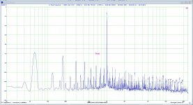
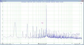
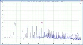
In the meantime, I got curious and did some measurements with that ES9038Q2M board from Breeze Audio. I tested the board with several opamp chips using the same setup. I include just three results here for illustration: JRC5532 (the original chip sent with the board), PBA2604 (from Academy Audio), and a dual AD797 (set on an adapter board).
All three results show the THD+N below -90dBFS, which is quite far from -120dBFS, but much better than -70dBFS. The graphs demonstrate substantial power supply induced noise that dominates the results. It's amazing how much noise can a regular full wave rectifier create!
It appears, however, that the THD+N tests do not tell much about the difference in audible sound quality. The JRC5532 actually measures a bit better than the PBA2604, but sounds the worst of three. I would love to hear your opinion on the PBA sound, if you find some time to try it.
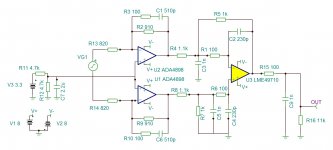
With a 3-opamp output stage and everything else done properly, ES9038Q2M can reach a -120dBFS distortion level. With a one opamp output stage like you have now it has to operate in voltage mode which increases distortion to closer to -70dBFS. That's a huge difference, of course.
Markw4, thank you for your valuable suggestions. I will definitely try the 3-opamp output stage as the next step, perhaps with lower resistor values in the differential amplifier than the post #3003 suggested.
In the meantime, I got curious and did some measurements with that ES9038Q2M board from Breeze Audio. I tested the board with several opamp chips using the same setup. I include just three results here for illustration: JRC5532 (the original chip sent with the board), PBA2604 (from Academy Audio), and a dual AD797 (set on an adapter board).
All three results show the THD+N below -90dBFS, which is quite far from -120dBFS, but much better than -70dBFS. The graphs demonstrate substantial power supply induced noise that dominates the results. It's amazing how much noise can a regular full wave rectifier create!
It appears, however, that the THD+N tests do not tell much about the difference in audible sound quality. The JRC5532 actually measures a bit better than the PBA2604, but sounds the worst of three. I would love to hear your opinion on the PBA sound, if you find some time to try it.
Attachments
I will definitely try the 3-opamp output stage as the next step...
Someone posted a similar 3-opamp output stage schematic from a Topping board that might actually be little bit better. Copy attached below.
I would still suggest that OPA1612 is the best opamp for the job. If it doesn't sound best it usually means there are other problems with the dac or power supplies that still need fixing. I would suggest to mount the output stage as shown in the instructions at: Dropbox - Output Stage Instructions.zip - Simplify your life
... loosely twisting the dac outputs for each channel together and running them along the ground plane down to the output stage is pretty effective for removing residual RF coming from the dac chip (a few pf of incidental capacitance to ground can be helpful, but not too much capacitance there or it sounds and measures worse). Helps keep opamp distortion lower that way and helps prevent heating of opamps from RF, IME.
In addition to a proper output stage, AVCC powering is critical for good sound quality. The AVCC power schematic at post #3003 is still good, although some people have substituted LT3042 or LT3045 as the low noise reference for the opamp buffers. In that case the LT304x should not be used to power anything else. Probably not necessary to use film caps for opamp output filter, average quality electrolytics are probably fine for that. AD797 makes a very good AVCC buffer
Don't know about PBA2604, can't find a link for it.
EDIT: one more thing: The voltage divider for Vref in the Topping schematic and in the post #3003 schematic shows Vref set equal to AVCC/2. That may not be optimal for minimizing distortion. The voltage divider resistors (R11, R12 for topping) can be adjusted to bring the quiescent I/V output voltage down to ground which is also something that can be done for AK4499. Seems worthwhile if starting from scratch.
Also, use good quality .1% or better resistors such as Susumu and NPO/C0G caps in output stage signal path. Bypass caps should be X7R.
Attachments
Last edited:
I'm using LT3045 feeding a LipoFe4 cell for each side. The problem is that the original potmeter is extremely sensitive on the regulator board. I found out that I could solder a 33.2K resistor instead of the pot but its really difficult at this point since everything is so tightly soldered together on the dac board. The offset is about 0.05V. Is this hearable?
The offset is about 0.05V. Is this hearable?
I very much doubt it.
Don't know about that power scheme though. For whatever interest it may be: Allo used a well filtered LDO and super caps for Katana AVCC, but used a number of SMD film caps of staggered sizes in parallel with the super caps too. Worked pretty well, but not sure if better than a good opamp buffer type supply. Changing that would have been one of the things I tried if I ever decided to get deeper into Katana.
Thanks for that feedback Mark! The psu I made is only to satisfy my own curiosity It has a 9 ohm resistor in series between LDO and battery&dac making it an high impedance LDO. That value was chosen for several reasons, but mainly the resisors won't burn up if the battery gets discharged somehow and regulator apply full charging current to battery. This allows me to use small resistors keeping the wiring extremely short. I've been following battery experiments on a youtube blog showing that a battery often has a huge capacitance component to them. And my half baked idea is that some of the transient voltage overshoot from the LDO will be dampened by the resistor in series. The battery I'm using has crazy low impedance and only a few mm of wire connects them to the dac chip. I think most battery systems fails because of several centimeters of wires and connectors. The idea is that the battery should be the psu, and the LDO is only there to make coarse adjustments.
To me it seems that many people like a battery solution better than a regulator solution so I therefore I wanted to try it. As a side note I found that the AVCCR drains some current when the dac chip should be off.. AVCCL doesn't drain anything at all.
It has a 9 ohm resistor in series between LDO and battery&dac making it an high impedance LDO. That value was chosen for several reasons, but mainly the resisors won't burn up if the battery gets discharged somehow and regulator apply full charging current to battery. This allows me to use small resistors keeping the wiring extremely short. I've been following battery experiments on a youtube blog showing that a battery often has a huge capacitance component to them. And my half baked idea is that some of the transient voltage overshoot from the LDO will be dampened by the resistor in series. The battery I'm using has crazy low impedance and only a few mm of wire connects them to the dac chip. I think most battery systems fails because of several centimeters of wires and connectors. The idea is that the battery should be the psu, and the LDO is only there to make coarse adjustments. To me it seems that many people like a battery solution better than a regulator solution so I therefore I wanted to try it. As a side note I found that the AVCCR drains some current when the dac chip should be off.. AVCCL doesn't drain anything at all.
- Home
- Source & Line
- Digital Line Level
- ES9038Q2M Board