Looks that I am first whor rides double bootstrapped hawksword casocde over the vssa's front end 
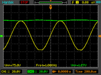
In double bootstrapped version (beta 1) psu voltage isn't wasted, output is nice swinging rail to rail. THD at very high load are going up to 0,03-0,05%.
Prapobly not bootstrapped vas would behave better, but it will waste some of psu voltage. Board is universal enough for both versions so I will try them anyway.
Attachments
Last edited:
Thanks Machina.
I was wondering why always amp has to be as perfest as possible, maybe the ''nice'' not allways natural sound is somwhere else. I remember some of my erly prototypes were sounding really ok even if measurements werent perfect.
So I will try to discover this subject a bit deeper.
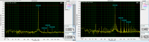
I just changed two resistors in my next prototype and yyyyyyy no it is not SKA GB150 belive me. This is still vssa based fet-hex amp.
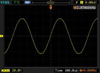
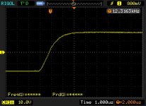
Look at the distortion profile. This time we are building high distortion amp
It sounds really good.
I was wondering why always amp has to be as perfest as possible, maybe the ''nice'' not allways natural sound is somwhere else. I remember some of my erly prototypes were sounding really ok even if measurements werent perfect.
So I will try to discover this subject a bit deeper.
I just changed two resistors in my next prototype and yyyyyyy no it is not SKA GB150 belive me. This is still vssa based fet-hex amp.
Look at the distortion profile. This time we are building high distortion amp
It sounds really good.
Attachments
Last edited:
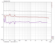
I did not tested lm334 but i think that ccs in this case doesnt have to be ''super duper'' cause it is loaded with 1000uF (more less) capacitor so in my opinion there not much diffrence between ccs type.
Basic version with resistors instead ccs was showing 0,00x% thd so as ccs version.
Basic version with resistors instead ccs was showing 0,00x% thd so as ccs version.
Hi Folks
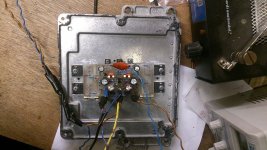
I built Amplifier based on Borys HEXFET Schematic.
Picture here:

Unfortunatly i am getting some crazy DC voltage on the speaker outputs (-26Vdc)
I recall a schematic with voltages over various components on it some where in this thread but i have went through it twice now and i cant find it. Can someone point me in the direction of where the schematic is that has measurements on it so i can correlate? Unless i am confused with another thread
Many Thanks
Cheers
Dom
Nice!
I've got some N-channel IRFP250N only.
Could anyone draw a variant of this circuit to fit only N-channel hexfet outputs?
Thanks!
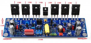
my design L150W .
it use IRFP250 *6
+ -70V,
Attachments
domyboy
Please check If you have all parts values correct.
Check if resistance values in current sources are correct (negative side there is resistor, on the positive rail there is resistor parallel with pot).
If values are correct than, try to adjust bias at output transistors (there should be around 7-7.5V across the N and P gates to get the mosfets biassed).
Than raport please.
ljm
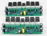
Very nice boards, compact desing, will fitt in small enclosure.
Please check If you have all parts values correct.
Check if resistance values in current sources are correct (negative side there is resistor, on the positive rail there is resistor parallel with pot).
If values are correct than, try to adjust bias at output transistors (there should be around 7-7.5V across the N and P gates to get the mosfets biassed).
Than raport please.
ljm
Very nice boards, compact desing, will fitt in small enclosure.
domyboy
Please check If you have all parts values correct.
Check if resistance values in current sources are correct (negative side there is resistor, on the positive rail there is resistor parallel with pot).
If values are correct than, try to adjust bias at output transistors (there should be around 7-7.5V across the N and P gates to get the mosfets biassed).
Than raport please.
ljm
Very nice boards, compact desing, will fitt in small enclosure.
Thanks Borys.
I have the left channel working. The right channel is proving difficult.
I have replaced Q8,Q7 & Q11 and then I replaced Q1, Q2, Q3, Q4, Q5 & Q6.
The working channel has -2.9Vdc before R22. The non working channel has +3.6Vdc there.
The working channel has -3.5Vdc before R21. The non working channel has +3.4Vdc there.
I have checked all the resistors all are very close to thier ratings.
I have inserted voltages on to schematic below:

Last edited:
my design L150W .
it use IRFP250 *6
+ -70V,
Thank you, ljm_ljm.
But is this circuit for sharing? Remember this is an open community, so we're looking for public domain stuff.
domyboy
On the lower driver Q7 you have +3.4V --> there should be -3,4V.
Looks like there is no bias at the output traniies --> am I right ?
Try to replace 3.3k resistor in Vbe with 2.2k and try to readjust the amp.
Hi Borys
I replaced R13 (3.3k) with 2.2k and then 1.5k and both made no difference.
I replaced R14 (4.7K) with 3.3k and then 1.5K and both made very little difference. 0.5Vdc on speaker output rather than 0.79Vdc before. 4Vdc on R22 driver and 3.8Vdc on R21 driver.
I also changed TR2 with a 5K trimmer but turning it full and then zero made no difference either which is really confusing.
Any other ideas?
Thanks
Dom
- Home
- Amplifiers
- Solid State
- FET-hex explendit amplifier