Here goes. This version is still with ideal CC's though, but it shows the performance of the circuit regardless. Here the THD logs:
THD 1K, 20 Harmonics
THD 20K, 10 Harmonics
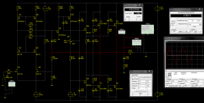
This is the base design I'll be working from. The next step is to work on real current sources, tune them and then prepare for a first build.
Here's the schematic. Note the hi-powered inputstage with a symmetrical 10mA for each half. Coupled with a 2-stage VAS and 2-stage output, each intermediate load to the previous stage is near neglible allowing it to retain its low THD figures throughout the stages, along with a 100dB+ SINAD.
THD 1K, 20 Harmonics
Code:
Fourier analysis for $out:
DC component: -5.8012e-005
  No. Harmonics: 20, THD: 1.88779e-005 %, Gridsize: 512, Interpolation Degree: 1
Harmonic Frequency    Magnitude    Phase        Norm. Mag    Norm. Phase
-------- ---------    ---------    -----        ---------    -----------
 1       1000         34.6474      -0.026254    1            0
 2       2000         2.5091e-007  145.778      7.2418e-009  145.804
 3       3000         8.58412e-007 129.397      2.47756e-008 129.423
 4       4000         2.05713e-007 129.21       5.93733e-009 129.236
 5       5000         1.38867e-007 -169.34      4.00801e-009 -169.31
 6       6000         2.06661e-007 129.715      5.9647e-009  129.742
 7       7000         2.55832e-007 98.1684      7.38387e-009 98.1947
 8       8000         2.11782e-007 134.395      6.1125e-009  134.422
 9       9000         4.44314e-007 165.093      1.28239e-008 165.119
 10      10000        2.61696e-007 138.826      7.55311e-009 138.852
 11      11000        1.37959e-006 -47.75       3.98181e-008 -47.724
 12      12000        8.79048e-007 148.363      2.53712e-008 148.39
 13      13000        5.60239e-006 -70.337      1.61697e-007 -70.311
 14      14000        8.83882e-007 62.1768      2.55108e-008 62.2031
 15      15000        2.49077e-006 -102.83      7.1889e-008  -102.8
 16      16000        2.59529e-007 73.849       7.49057e-009 73.8753
 17      17000        4.72164e-007 43.8352      1.36277e-008 43.8615
 18      18000        2.11127e-007 80.5477      6.09359e-009 80.574
 19      19000        2.76139e-007 119.155      7.96997e-009 119.181
 20      20000        2.03156e-007 88.8985      5.86353e-009 88.9248
Code:
Fourier analysis for $out:
DC component: -1.2406e-006
  No. Harmonics: 10, THD: 8.4441e-005 %, Gridsize: 256, Interpolation Degree: 1
Harmonic Frequency    Magnitude    Phase        Norm. Mag    Norm. Phase
-------- ---------    ---------    -----        ---------    -----------
 1       20000        34.6396      -0.5252      1            0
 2       40000        1.05821e-005 -163.41      3.05491e-007 -162.88
 3       60000        1.20487e-005 6.71502      3.47832e-007 7.24022
 4       80000        2.59868e-006 47.0909      7.50205e-008 47.6161
 5       100000       2.30448e-005 -1.0305      6.65272e-007 -0.50532
 6       120000       2.88365e-006 101.762      8.32472e-008 102.287
 7       140000       1.4804e-006  58.3999      4.27373e-008 58.9251
 8       160000       3.0348e-006  90.8256      8.76108e-008 91.3508
 9       180000       3.16436e-006 4.91236      9.13508e-008 5.43756
 10      200000       5.5557e-006  90.7983      1.60386e-007 91.3235
This is the base design I'll be working from. The next step is to work on real current sources, tune them and then prepare for a first build.
Here's the schematic. Note the hi-powered inputstage with a symmetrical 10mA for each half. Coupled with a 2-stage VAS and 2-stage output, each intermediate load to the previous stage is near neglible allowing it to retain its low THD figures throughout the stages, along with a 100dB+ SINAD.
Attachments
Very nice design! lnly with vas and two source follower you loose twice 8 volt of drive is 16 volt, this is always with source followers, maybe a vas with a drain follower will help, but it is not so bad because you have plus minus 50 volts supply.
It is easy to make this supple 16 volt higher for the vas and the input jfet because of the use of cascades.
Maybe I am wrong I am not so a calculate man, more a practice man.
It looks very good that is a fact, simple and elegant.
It is easy to make this supple 16 volt higher for the vas and the input jfet because of the use of cascades.
Maybe I am wrong I am not so a calculate man, more a practice man.
It looks very good that is a fact, simple and elegant.
Thanks!
The voltage drop due to Vgs of the source followers is no problem to me; while not shown in this design, I always run the output stage on its own supply to retain efficiency while having plenty of voltage to work with. The output stage in this schematic would still yield ~1ppm THD when running on a reduced output supply of ~ 45V each rail. The Vgs drop isn't all that spectacular though, the ECX's already start conducting with a Vgs as low as a few hundred millivolts.
The voltage drop due to Vgs of the source followers is no problem to me; while not shown in this design, I always run the output stage on its own supply to retain efficiency while having plenty of voltage to work with. The output stage in this schematic would still yield ~1ppm THD when running on a reduced output supply of ~ 45V each rail. The Vgs drop isn't all that spectacular though, the ECX's already start conducting with a Vgs as low as a few hundred millivolts.
The voltage drops are in the irf and the output fets, the other are drain followers and yes then you have no problem.
it is indeed easy to make solution by give the input stage more supply, this time some more then normal with mosfet amp, output stage has to be lower then driver stage for drive full potention of output.
You have done clever work, I have on this site some like it with balanced al mosfet amp but I am to busy to go on with that now, first my hybride who works very nice and clean already but not so low THD, so I will some day build yours and listen to it, do you break now the feeback rule that it sound worse as without it, well I now that current feedback don,t, it is more complicated to get stable offset.
so lets rock the boat ;-)
Yeah I'm definitely going to build this one after I got the initial setup done completely in the sim. Once sitting on a dev board, I'll continue cross optimizing between reality and sim to further improve it ")
I currently have a design sitting near completion though its performance doesn't even get close to this new design. Fun thing though is that it performs better in real than it does in the sim But there I did the same. Initial design in sim, cross-optimizing between sim and real after having built the initial version.
I currently have a design sitting near completion though its performance doesn't even get close to this new design. Fun thing though is that it performs better in real than it does in the sim
But there I did the same. Initial design in sim, cross-optimizing between sim and real after having built the initial version.I have multisim so I wil test it some time if you alowed me, I am a hybride man with valves and mosfets but it is always interesting to test also solid state full mosfet amps , there are also more and more mosfets who are perfect for this.
and the sound, well, so many ears so many posibilities, ;-)
and the sound, well, so many ears so many posibilities, ;-)
I like the FET-buffered FET VAS. This should greatly isolate the distortion of the output stage. I wonder if this is one of the reasons for the low distortion.
The output-inclusive miller compensation is intimidating but I suspect you have done this before without difficulty.
It is simple to put a 470k resistor and reverse protection diode (to model CCS semiconductor capacitance) to see how good a CCS will be needed in that position.
Have you checked the ECX models for consistency with real life? I found these models to give overly optimistic switching behavior because the gain curve was too smooth. I use Cordell's FET models now.
- keantoken
I've found it to be a minor reason. The biggest jump came from significantly increasing the IPS current, up to 10mA for each JFET. I specifically designed its CCS to reference the JFET sources to keep their Vds the same even with a moving input signal. That's why the 25mA source also sinks the 5mA CCS bias.I like the FET-buffered FET VAS. This should greatly isolate the distortion of the output stage. I wonder if this is one of the reasons for the low distortion.
This is a thing that particularly originates from reality. In the sim they do nothing, but in real it completely muffles the parasitic oscillations in the output devices that would otherwise exist with such low gate stoppers. The ECX'es would oscillate up to 80MHz. I've applied this to my current design as well.The output-inclusive miller compensation is intimidating but I suspect you have done this before without difficulty.
I find them to be pretty alright as for slope smoothness goes. The one thing that's lacking from the models are the parasitic inductances. I feel this is a mandatory attribute to simulate to find unwanted oscillations. The IRF datasheets state the wire inductances. Not so for the ECX'es so that would be some guess work. Or apply the 47pF local feedback that's proven to workIt is simple to put a 470k resistor and reverse protection diode (to model CCS semiconductor capacitance) to see how good a CCS will be needed in that position.
Have you checked the ECX models for consistency with real life? I found these models to give overly optimistic switching behavior because the gain curve was too smooth. I use Cordell's FET models now.
Today I may work on the current sources. I'm going to try to make those all FET too.
Okay guys, MacGyver time. I put together this simple but effective square wave generator. It can also provide triangle output from across the timing capacitor, which could be diode-shaped into a sine. Anyways, it is super fast. Theoretically, if your rise time is fast enough, it won't matter if there is some overshoot because your circuit will be too slow. It had about 5% overshoot the way I built it, which I think is pretty good with a 15nS risetime. With better transistors and a direct scope connection it should be faster.
- keantoken
- keantoken
Attachments
MagicBox
I would consider using lateral Mosfet as drivers too. 2SK213/j76 are IMHO fra better than IRF510/9510.
Koldby
I can try with them but I don't have models for those. I'd assume Cordell made models for these?
The reason why I picked hexfets as drivers is because of their steep Vg/Id curve, further minimizing VAS loading by the output stage. Of all the IRF hexfets used as drivers/cascodes I found the 510/9510 pair to perform the best but if you want to exceed 100V then you'll have to settle for a 610/9610 pair.
It takes time to make accurate models, so Cordell hasn't gone out of his way to make a lot of them. They are here:
CordellAudio.com - SPICE Models
- keantoken
CordellAudio.com - SPICE Models
- keantoken
Magicbox,
My congrats, very well thought out amp, finally another has seen the light and the advantages of using fets in buffered vas. The disadvantage lies that high frequency distortion (usually after about 3 Khz) is higher than would be if you used BJT but the sound to my opinion is improved. However if you are interested in further improving THD figures look at microprocessor design techniques of the last 10 years and with a little imagination youll find a way to further improve performance, this in special attention to bettering high frequency (also Lower frequencies) THD to levels superior than that achieveable by BJTs. Sorry I cant say more as the audio company I sold the concept and design would reprimand but no damage done if someone else happens to find the way as no patents issued in analog or digital domains as far as I m aware of. It also improves bandwith and thermal issues (memory distortion as it is known here) and only 2 minor caveats.
I adopted this type circuit about 15 years ago but minor differences, ltp cascodes not referenced to ccs, at first with Bjt inputs, Bjt cascodes when using Jfets, different compensation scheme, the use of bjt mirror and laterals driving BJT outputs. Then about 9 years back I started using the new vas concept. My motivation stemmed from Val Alstine´s patent regarding the use of mosfet as emitter follower preceding the vas from 1987, I wanted a way to use the mosfet as I saw and heard advantages but didnt want to infringe on the patent and ended up with only mosfets in vas. THD was slightly worse at very high frequencies than Pioneer M90 -91 which was the circuit I wanted to better as a reference back in early 90s and had the lowest THD20 (claimed in company publications) figures I was aware of. Beware that simulation results especially at high frequencies might be a little more optimistic than with BJTs as mosfet models are pretty bad when modelling the subthreshold and weak inversion regions as well as Cgd and Cgs.
All in all, excellent, you should be happy with the performance and sound if you pursue to build.
@kees52 - what about using CSS + LED referenced to lower fet source instead of voltage divider for cascode biasing?
Sorry it was to @MagicBox
@homemodder:
Thanks for the kind words man. So by using a source follower FET I'm actually infringing on a pattent? That's an amusing thought. I've done nothing more than applying logic, using known circuits. Anyways, what I'd really like to do is to change this amp into a full symmetrical version by mirroring this schematic and create a push/pull VAS. I have yet to find suitable PJFETs for the negative going LTP. For everything else I have workable P variants.
I suspect the amp's THD figures will either stay the same or improve a bit but the primary reason is that right now, the slew is highly assymetrical. If you'd look at a square wave you'd think "that can NEVER sound good" lol. That's one reservation I have about this amp. It follows sines like a charm, but its transient response does not meet my desires. I'm hoping to fix that by going fully symmetrical like my previous design. But that one had BJTs for the IPS and VAS.
@barmanekm: You mean the bias for the BS170's? I didn't want to use a zener to have them bias'ed about 8V above the SK170 drains and thus went with a regular resistor. LED Vdrop would be too few unless I would put like 3 leds in series to obtain the desired bias voltage.
I however do plan on using LED references for the LTP and driver CS, each cascoded with a suitable FET.
@homemodder:
Thanks for the kind words man. So by using a source follower FET I'm actually infringing on a pattent? That's an amusing thought. I've done nothing more than applying logic, using known circuits. Anyways, what I'd really like to do is to change this amp into a full symmetrical version by mirroring this schematic and create a push/pull VAS. I have yet to find suitable PJFETs for the negative going LTP. For everything else I have workable P variants.
I suspect the amp's THD figures will either stay the same or improve a bit but the primary reason is that right now, the slew is highly assymetrical. If you'd look at a square wave you'd think "that can NEVER sound good" lol. That's one reservation I have about this amp. It follows sines like a charm, but its transient response does not meet my desires. I'm hoping to fix that by going fully symmetrical like my previous design. But that one had BJTs for the IPS and VAS.
@barmanekm: You mean the bias for the BS170's? I didn't want to use a zener to have them bias'ed about 8V above the SK170 drains and thus went with a regular resistor. LED Vdrop would be too few unless I would put like 3 leds in series to obtain the desired bias voltage.
I however do plan on using LED references for the LTP and driver CS, each cascoded with a suitable FET.
Symetrical has disadvances I am told, look on my topic who has symetric vertical amp, I have tested it and it sounds wel, but single end driving sounds better, a lot, special the rest in music and the relaxing warm sound, it is my experience with hybride tube amp, a dc coupled one I have here somewhere, I have drawn your design in multisim, even with 30Khz the THD is very very low, so test this version first, I don,t think it wil better with symetrical versions, mosfets are not so wel matched.
Your design you now have is promising, don,t be afread of patents, most are gone.
http://www.diyaudio.com/forums/solid-state/194179-jfet-input-mosfet-vas-vertical-output.html
Last edited:
Going with a push/pull VAS I don't think I could get away with using MOSFETs only. The nice perc of a tranny is it's BE junction which allows resonable accurate control of quiesent current. Using FETs biasing the VAS is possible but would require error and trial biassing. It also leaves too much uncertainty due to Vgs differences amongst same models. So yeah, for now I'll stick with this design and finish up the current sources. I'm still in debate whether to use BJTs for current control or JFETs. Once completed I'll draft up a PCB for the first real-world tests
P.S. am going to hunt for models of the 2SK213 and 2SJ76 laterals and see if they perform better than the IRFs in this particular case.
P.S. am going to hunt for models of the 2SK213 and 2SJ76 laterals and see if they perform better than the IRFs in this particular case.
Last edited:
- Status
- This old topic is closed. If you want to reopen this topic, contact a moderator using the "Report Post" button.
- Home
- Amplifiers
- Solid State
- JFET input, MOSFET VAS, LATERAL output = Perfect!!