To extend the adjustment range in the buffer manipulate the value of R21 - lower it if you need more current to match the current through BF862.
If you measure the voltage over R16 you can calculate the current through JFET - the CCS (Q6, Q8) should deliver the same current which is I = Vbe(Q8) / (P2+R21)
See posts #359 - #365
If you measure the voltage over R16 you can calculate the current through JFET - the CCS (Q6, Q8) should deliver the same current which is I = Vbe(Q8) / (P2+R21)
See posts #359 - #365
Last edited:
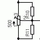
I have some 500 ohms trimpots,are they to much to use in the preamp?
You can use them, but add 2 lower value resistors (220R - 330R) as R10,R11 here:
Attachments
Last edited:
Been running the LSK all night and as it becommes warm it is quite stable,(within 20mV).
But I´ve noticed another thing as I turn it off the offset goes up to about 1,2v...
I guess that can be fixed with a relay on the output.
But what about if I put caps after the buffer what values should they be?
But I´ve noticed another thing as I turn it off the offset goes up to about 1,2v...
I guess that can be fixed with a relay on the output.
But what about if I put caps after the buffer what values should they be?
... if I put caps after the buffer what values should they be?
It depends on input resistance of the next stage (power amp) - if it's 10k, use 10uF, for 100k use 1uF and so on...
Juma, in order to have a tighter offset control, do Q1-Q3 & Q2-Q4 have to be thermally coupled or Q1-Q2, referring to schematic in post # 66?
The same component designations and my question above also applies to schematic in post # 118.
I am half way through a PCB layout. Thanks.
The same component designations and my question above also applies to schematic in post # 118.
I am half way through a PCB layout. Thanks.
Juma,
I would like to build Line Amp as per post #66 and Pos #271 but without buffer.
Line Amp to be use to drive standard Power Amplifier.
The Line Amp will suplly with 26 VDC, because my transformer 24 VAC CT.
Please advise if the schematic attached is correct as well as the value of components.
2SJ74 and 2SK70 V grade hard to find in matching right now, only possibly 2SJ74 and 2SK70 BL grade.
If possible to parallel 2SJ74 and 2SK70 BL grade in onder to achieve 2SJ74 and 2SK70 V grade .
Your kind advise is highly appreciated.
Rgds,
Sun
Attachments
Sunami,
your sch. is problematic:
- P2 is way to low (50k would be realistic value)
- your outputs should have same voltage output, meaning approximately the same resistance to ground (the way you drew it, negative output will give higher voltage)
- you don't need double JFETs, adjust CCSs accordingly (Idds-20% for JFETs + 10mA for BJTs)
Juma,
Thank you for your suggestion.
I just copy paste the two schematics of post #66 and Pos #271.
Attached schematic might be correct or incorrect.
According to datasheet Idss BL grade : 6 - 12 mA.
I need your help to calculate correct value of components or inform me the formula,
because my knowledge inadequate to avoid wrong calculations value of components.
Best regards,
Sun
Attachments
... I just copy paste the two schematics of post #66 and Pos #271....
You can't "just copy/paste" two different circuits.
Sch. from post #66 is a standard preamp with gain of about 9V/V and the sch. from post #271 is a phase splitter for balanced drive with gain of a bit less than 1V/V per phase (about 6dB differential).
You have to decide what you want/need - you can't have both at the same time with this circuit (without duplicating it)...
To answer please answer this first:...
I decide to use schematic Post #66 without buffer.
supply with 26 VDC and 2SJ74 and 2SK70 BL grade.
Please advise any change value of components.
...
1. What's the Idss of your Toshiba JFETs ?
2. How much gain do you need (you can't go crazy here since you don't wan't a buffer) ?
3. How much output voltage swing you need (be specific - Vrms, Vpeak or Vpeak-to-peak)?
4. What's the input impedance of your power amp ?
5. Do you want to use resistors (R4, R5 in sch. in post #66) or CCS in their place (like you proposed in your sch.) ?
Dear Juma,
I try to answer your question as below.
1. Toshiba JFET still in supplier, I have not order yet until I have confirmation from you.
2. Standard preamplifier gain maybe 20 dB, I not quite sure.
preamplifier with input source DAC.
Can I use buffer supply voltage same as Line Amp (26 VDC)
3. 9V/V is OK.
4. 47 K.Ohm (Hafler DH-220 Modified by Musical Concept)
5. I prefer CCS if possible.
Best regards,
Sun
- Home
- Amplifiers
- Pass Labs
- LSK pre - BAF 2013