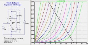
Rd is the "triode" drain resistance, not the output load RL. Rd=μ/gmJ1. See https://www.electronics-notes.com/a...s/triode-valve-vacuum-tube-formula-theory.php
Yes, there is an inconsistancy in the labelling of the MOSFET in the figures and the equations. M1 and M2 refer to the same MOSFET.
Yes, Rk is the resistance of R3+R4
Yes, there is an inconsistancy in the labelling of the MOSFET in the figures and the equations. M1 and M2 refer to the same MOSFET.
Yes, Rk is the resistance of R3+R4
Granted, but this {(1-k)*Rk} and {k*Rk} [aka R3 & R4] are creating a VgsM2 on their own already, {Vcasc} only lifting VG2 higher then intended!
And what if {Vcasc} is omitted and the lower side of {k*Rk} is connected to S1 (node 'above' {Rs}), the source of J1? (feedback?)
I'd say: simplify - it does not appear in the equations either (obvious, though).
And what if {Vcasc} is omitted and the lower side of {k*Rk} is connected to S1 (node 'above' {Rs}), the source of J1? (feedback?)
I'd say: simplify - it does not appear in the equations either (obvious, though).
This would cause the MosFET gate voltage (G2) to follow the D2 voltage directly (schematic in post #9), very similar to the "pentode" cascode shown in the first post. Adding the Vcasc voltage offsets the G2 voltage, which obviously makes the whole thing behave in a "triodey" way.what if {Vcasc} is omitted and the lower side of {k*Rk} is connected to S1 (node 'above' {Rs}), the source of J1?
I guess @lhquam will have a better explanation.
That offset is required to preserve the "shape" of the triode curves. To obtain a 10X expansion of the Vds range, k must be around 1/10. Consider the "pentode" case, where k=0. Without the Vcasc offset, there would be no idle current.
Be patient, a more complete explanation is underway.
Be patient, a more complete explanation is underway.
Maybe this will help:
- Start with the Vcasc needed when k=0, the "pentode" condition. Adjust Vg and Vcasc to obtain the desired idle current and Vds[J1].
- Increase k slightly, and readjust Vg and Vcasc to obtain the desired idle current and Vds[J1]. The changes to Vg and Vcasc should be relatively small, roughly proportional to the change in k.
When k=0, {(1-k)*Rk} [::R3] is R3 and {k*Rk} [::R4] is 0 (zero), rendering into a 'pentode' configuration as {Vcasc} prohibit Vd2M2 from changing the G2M2 node. Adjusting Vg (assumed Vg1) and {Vcasc} aka Vg2=Vd1 determines the desired Id (J1) in the ohmic region (ok).
As soon as k ≠ 0, R4 exists and will be part of the equation of (Vd2 -Vcasc) over the R3/R4 divider. And yes, in some respect proportional to the k factor indeed. But as k cannot be 0 for this application, Vcasc has become superfluous instantaneously.
I do follow your thoughts, I do admit the viability of this configuration. Actually, it is great! But Vcasc is a mindtrap.
Are you suggesting totally discontinuous behavior when k becomes just slightly non-zero?Vcasc has become superfluous instantaneously.
I suggest you try some simulations of the circuit.
Perhaps this image will help explain Vcasc.
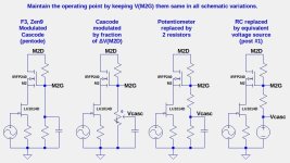
The left schematic shows a fragment of the F3 (or Zen9) modulated cascode which has a voltage divider between M2D and ground with a large capacitor across the lower resistor.
In the remaining schematics the cascode is modulated by a fraction of the AC voltage of the drain of MOSFET M2,
with the 4th schematic being that of post#1.
In all variations, the quiescent (idle state) voltage at M2G is the same, maintaining the same operating point (bias current and LU1014 Vds).
Attachments
Last edited:
Don't destroy theory by data.
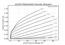
Don't worry. I built the modulated cascode circuit as described and gave it to my curve tracer. Once the magic smoke was out, and new parts were in, the curves looked as in the attachment. Pretty cool!
Did I just build a holy grail?
Don't worry. I built the modulated cascode circuit as described and gave it to my curve tracer. Once the magic smoke was out, and new parts were in, the curves looked as in the attachment. Pretty cool!
Did I just build a holy grail?
Attachments
Last edited:


Holly Grail is KT90, having Ultralinear curves pretty much all at 45degs
") How about the 300B?
How about the 300B?
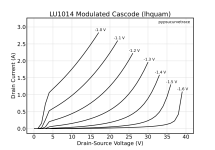
See measured curves in the attachment. There is something funny going on a low voltages, and the curves are compressing at high voltages.Here are even better triode curves with Rs eliminated (Rs=1m). Be very careful to limit the current range or will will have more smoke.
Well, the LU is a SIT, but it's cheap and abundant. I am not concerned about oscillation, since my build is a rat's nest with looong wires and looooops. It seems to behave ok.Poor man's SIT, with an easier gate to drive.
..... if you can keep the oscillation under control.
Attachments
I am not sure what you mean by "clipping in" and "full circuit". Can you explain?you would be clipping in the full circuit.
- Home
- Amplifiers
- Pass Labs
- LU1014D Modulated Cascode