Hi.
I could use some help with a little fault-analysis.
I have a working classD that have played several hours with a ohmic load. PSu is +/-70V. load 4-8Ohm. Mosfets are IRF640N. Driver iR2184. Drive si 10Ohm with a schottky in parallel. NO zener across the gate. Switching is around 300Khz iddle. Filter is 15uH/1uF. I'm very sure that the IRF640 are real and not fakes
PSU is a regulated LLC of my own design.
Without a load the output of a pre-filter-design can rise to very high levels. I think, I got that covered with a little PFFB.
I ran this little test twice yesterday with the same result:
Amp was running idle with no load and everything was ok. I was touching the input to "provoke" it a little and voltage-swing on the output gets close to rails. Current-draw very low.
BUT, if hum-pickup from touching the input rises above some level, the output-voltage also rises and at some point ( 1second with steady "hum-input) current-draw rises and both mosfets short out. They short totally internal zero ohm: GD, GS, DS.
This happens very, very fast before heat has time to build. Everything appear cool. Supprissingly the rest of the amp is fine and runs with a new pair of mosfets.
I saw a paper talking about an avalanche-related failure where the GS-voltage rose above max-rating because of inductive loads. The large GS-volatage turns on the mosfet and kills it with a total short.
I still have to test if it is some sort of bus-pumping that rises Vcc-Vss above the 200V-rating of the IRF640n.
What else to test? - any guesses on the root-cause?
Is it normal for mosfet to short totally like this when its apparently not due to heat?
Deadtime?
100ohm on gates is a bit high if deadtime isn't very long. Rather start with 10ohm and no parallel diode and optimize from there. The GS voltage is better controlled with Rg 20ohm or less, preventing erronious GS voltage. I think the avalanche event u refer to only applies to DS, not GS, GS being very sensitive to over voltage and having no inherent avalanche protection...?
Or are u using the high drive resistance to slow the turn-on, then the diode for fast turn-off, thereby creating deadtime in the process?
Deadtime?
100ohm on gates is a bit high if deadtime isn't very long. Rather start with 10ohm and no parallel diode and optimize from there. The GS voltage is better controlled with Rg 20ohm or less, preventing erronious GS voltage. I think the avalanche event u refer to only applies to DS, not GS, GS being very sensitive to over voltage and having no inherent avalanche protection...?
Or are u using the high drive resistance to slow the turn-on, then the diode for fast turn-off, thereby creating deadtime in the process?
it is 10(ten)ohm. But I can see that it looks like 100 in the post.
Gate-drive it self appears to be ok. It is running ok with a load and normal signals in.
The problem only appears with no load and big "random, hum/noise" input. I know this is a very bad condition for most classD's but I would like my design to be tolerant of this.
Yes, most references to avalanche is about the DS-voltage. But I saw somewhere a note about the spike becomming high and fast enough to charge the gate through the DG-capacitance. IF this happens I can see that a very fast destruction could happen?
Kind regards TroelsM
Can it be with out load the output filter inductor conducts current into the capacitor, and at some point the conduction stops or changes direction producing a large voltage spike?
The C-dg can turn on the device if a very fast dv/dt on V-drain. I have seen some place a small cap on G-S to shunt very fast edge signals on the gate to prevent this (in the tens of pF range). But I imagine this may slow things down too much and/or give high switching losses. I have yet to experience it so really cant say anything fruity. Do u have any means of measuring rise/fall edges in the lower nanosecs?
I would probe the output pre filter and look for spikes.
What about inserting a true signal, a sin signal. perhaps, touching the input causes the amp go in powerful oscillations. My humble PC amp has no zener in the gates, (IR2110) and no (expressly) dead time more than the IR internal generator. No problem since about 4 years ago.
Attachments


Hi.
I could use some help with a little fault-analysis.
I have a working classD that have played several hours with a ohmic load. PSu is +/-70V. load 4-8Ohm. Mosfets are IRF640N. Driver iR2184. Drive si 10Ohm with a schottky in parallel. NO zener across the gate. Switching is around 300Khz iddle. Filter is 15uH/1uF. I'm very sure that the IRF640 are real and not fakes
PSU is a regulated LLC of my own design.
Without a load the output of a pre-filter-design can rise to very high levels. I think, I got that covered with a little PFFB.
I ran this little test twice yesterday with the same result:
Amp was running idle with no load and everything was ok. I was touching the input to "provoke" it a little and voltage-swing on the output gets close to rails. Current-draw very low.
BUT, if hum-pickup from touching the input rises above some level, the output-voltage also rises and at some point ( 1second with steady "hum-input) current-draw rises and both mosfets short out. They short totally internal zero ohm: GD, GS, DS.
This happens very, very fast before heat has time to build. Everything appear cool. Supprissingly the rest of the amp is fine and runs with a new pair of mosfets.
I saw a paper talking about an avalanche-related failure where the GS-voltage rose above max-rating because of inductive loads. The large GS-volatage turns on the mosfet and kills it with a total short.
I still have to test if it is some sort of bus-pumping that rises Vcc-Vss above the 200V-rating of the IRF640n.
What else to test? - any guesses on the root-cause?
Is it normal for mosfet to short totally like this when its apparently not due to heat?
PSU is a regulated LLC of my own design. interesting.
1.) +/- 70V, IRF640N. Driver iR2184. Post your schematic. do some research on the forum why an IRF640N isn't suitable and at +-70V you playing with fire. I would recommend +/- 30V for testing with those ancient mosfets, irrespective fake or not.
2.) I have seen lots of a pre-stage RC networks (before the output filter) always has "some" type of load connected (especially if its a self oscillating amplifier), something like a 33R 1W and 100p capacitor to act as an output damper. (RC values dependent on under/over damping response)
3) Your signal input op-amp stage have a HF compensation network this is a must!
whats the gain set to? have you simulated behavior. differential is the way to go.
4) DT dead-time setting, series gate resistor, series diode, snubber(s), bus rail inductors with sufficient low esr capacitors. (all of this needs to be independently simulated)
5) Your drive circuit needs to be critically analysed no simple answer for such a in-depth topic many experienced here post amazing projects with very detailed work on how to build a successful project, fragmented knowledge.
Last edited:
These kind of failures do happen specially with high supply voltages. They often relate to poor body diodes of the MOSFETs - these create "tail currents" when hard switched off ("commutation") which occures with inductive load (output inductor!). I suggest to choose better PowerMOSFETs, not that true oldies.
Thank you for all the valuable input. I really appriciate it, although I'm not clever enough to understand it all.
First of all. This have been an on/off project for more than a year, but I'm no expert and I dont have the time or patience to read all the theory before I start ;-)
I did not get to this point by building a prototype and connecting it +/-70V for the first test. - that being said: I still have a ton to learn.
I have simulated a lot but not much on the actual mosfet behavior under max stress conditions. I realize that 350W@4ohm is bot the easiest target.
I have had the complete prototype running in a closed box with no air circulation and the hottest parts got to around 80degC. Thats with 70Vp over 4Ohm. It ran for hours.
I get that the IRF640n is old. But it was what I got and I wanted to keep it simple. Whats the cheap, availible alternatives?
There is NO shortcircuit-protection. Yes, it would be nice to have, but I had to stop somewhere. Its going into an active speaker so shorts are probably not the most likely fault.
Deadtime is fixed with Ir2184 and I think the heating of the mosfets corresponds pretty good with the expected I^2R heat from the current.
Last edited:


You should never run class d without a load.
The output filter will ring badly and have very high volts on it, much higher than the supply.
Blown mosfets can be from overlapping gate signals.
Or from shoot through from wrong deadtime.
Are you sure the output stage is the problem ?
If the gate driving signals are wrong that will blow up mosfets too.
Bus pumping can raise up power rails considerably and sometimes reach mosfet breakdown voltage. But this tends not to happen with music sources unless very bass heavy.
The power rails should be well decoupled with 100nf close to mosfets.
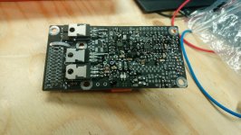
My impressions of the schematic, the MOSFET driver section:
Well its not the recommended circuit from the IR2184 datasheet is it? I can't see anything to stop Vb-Vs exceeding 12V (pins 8 and 6) as there is a dodgy looking leakage path from the HT via R30 and R32 to the Vb. That alone could pop the top MOSFET.
R52 strains the bootstrapping circuit by imposing a DC path to discharge the floating cap C24, which is clearly why R30 and R32 were added - alas that's not how these chips are designed to operate.
C24 needs to be ceramic multilayer to handle the high speed current requirements (dI/dt here can be of the order of 10^7 to 10^8 A/s). C24 only needs to be about 10 times the MOSFET input capacitance if there's no other load, but must be very low inductance, an electrolytic or film cap will not do. T5 and T7 are presumably designed to speed up switch off compared to switch on. This isn't likely to work (MOSFET gate driver chips can source and sink large currents - more than an amp in a fraction of the time T5 or T7 can switch off). Stored charge in these devices could be playing havoc with the switching. A simple schottky across R42 and R57 would not have this problem if asymmetrical was really important.
C22 and C24 need to be right on the chip's pins, a few mm away at most, and all the high speed high current gate path needs to be tightly laid out for minimum inductance, my favorite way is to route the gate current path over the returning source current path on a 2-layer board to minimize loop area and keep the fields mainly inside the PCB laminate.
If there is any distance between driver and MOSFET add a 15V protection zener across gate/source to clip any inductive ringing.
C21 looks totally wrong, the switching waveform needs to be crisp.
Last edited:
C21 looks totally wrong, the switching waveform needs to be crisp.
If there is a slow edge you could get into situation where both mosfets are on.
Another situation is where output clips and upper mosfet gate capacitor discharges and you end up with upper mosfet in linear region and dissipating lots of power.
There seems to be a misconception that a zener at the Vgs for clamping protects against high dv/dt , this is NOT true, the zener in question is used for slow gate Vgs signals, however here we anticipating to clamp signals in access of 100MHz leaking in and out from the power fets (via its parasitic capacitance) into gate and to the IR driver. The gate's thin channel will probably fail (no heat required here)
TVS high speed clamp diodes exists for this reason, but doesn't apply here, cause the currents in question are too high, it wont help with the real problem and there are many.
1) +/- 70V that IR + single transistor drive circuit is very mediocre.
2) LM311D PIN 7 and 6 can be connected together to improve propagation delay speeds.
3) The gate pull-down resistor 4k7 seems very low, 100k is fine.
5) Probably worse and most complex: The output has two loops, one post the other pre-feedback, here lies many problems and interesting research and improvements.
a) The carrier residual from the output (pre-stage) feeds directly into the input of the TL072, using poles and zeros lead/lag networks, you can actually simulate this independently in a simulator and see how she behaviors. The main thing I can see here is output before the filter has spectral content/noise way too high for that OPAMP to handle and probably results in failure line noise can even make it fail, who know what that network's behavior looks it, only a bode plot can show you. Consider researching compensation topics, Type I, II, III and get some understanding how important control stability is. The same goes for the post loop, only this time the loop is taken after the filter, so here too that loop needs to be analysed.
Part of your modulator design is very common in class-d car audio amplifiers, with failure at random like yours did, International Rectifiers first generation class-d prototype reverberates 10 years later.
Last edited:
Problems rise exponentially with supply voltage, so it might be helpful to start with lower supply voltage.
I love LTSpice, but it is not really helpful in predicting failures caused by excessive switching stress.
2 decaces ago I just struggled at this point.
My idea was a tough simulating program should burn a blind spot into the tube monitor when components fail - just to teach the stupid developper.
Wishful thinking until now😉
Problems rise exponentially with supply voltage, so it might be helpful to start with lower supply voltage.
I love LTSpice, but it is not really helpful in predicting failures caused by excessive switching stress.
Wishful thinking until now😉
Wrong:
That's cause you treating LTspice as a system level wide simulator (simulate the whole thing and wait a few minutes/hours/days for it to converge with results), obviously you cannot predict all failures, what do you think loop analysis is used for oscillating behavior only. detailed loop behavior under all load/idle/ short-circuit circumstances behavior, the experienced shown us on the forum this in great detail, I own one of their amplifier and its working to this day born from a LTspice simulation (see class-d lite project).
You can only improve what you don't understand by separating that as a single problem and breaking it into chunks to work with. This is more a how to problem solve and design exercise.
Last edited:
I venerate chocos work on the class-d lite amp, no doubt he plunged much deeper into theory than I did. I was talking about non-linear transient analysis, not linear AC-Analysis. The latter has been quite helpful for me, I use it permanently. Transient analysis including efficiency analysis have to be taken with a grain of salt as models of the semiconductors used are either unobtanium or inadequate to explore switching behaviour.
Certainly this is not a flaw of LTSpice but of the models available.
btw - I stand to the first of my statements you cited above.
Certainly this is not a flaw of LTSpice but of the models available.
btw - I stand to the first of my statements you cited above.
Last edited:
- Status
- Not open for further replies.
- Home
- Amplifiers
- Class D
- Mosfet failure analysis