Aaw too true, there's gotta be a balance!I was told once that relying on square waves leads to pushing the envelope too far in favor of a wide bandwidth v. a noise free circuit, but everyone is still doing it...
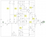
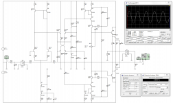
I've now prepared the schematic. It's large and most likely will not fit full-screen. You'll have to save it to your computer and view it unzoomed. The probe baloons show currents and voltage in the idle state. Component values are exactly as they are on the real prototype except for the transistors - they're all BC550C/560C. These were not available in the sim.
I'll follow up with a thorough explanation on its workings soon
May be an interesting thing to note is that it is a VFB circuit, there's no CFB at all.
Attachments
Last edited:
Well, are you guys ready for a book? *grins*
Here's the explanation as promised
The Basics
Under normal idle conditions, the VAS current is supposed to be a stable DC current. This means, both the N and P VAS devices conduct the same amount of current, keeping the output centered. When the input changes, the VAS action is to open up one device, while closing the other untill the output settles to the new value. This is commonly descibed as a push-pull action. The current variations in the VAS rail represent the error signal of the feedback system. Generally we can say that the current through the VAS devices will be a constant. This is the principle that is used to create and implement the auto-bias function of this VAS.
Where to start?
The easiest way to understand this circuit is remembering the mentioned principle while we start at the cascode devices Q9 and Q20 and work our way to the input of this VAS. We will assume a steady state VAS current of about 12mA. It's the cascode Q9 and Q20 that convert the current to a voltage. Devices Q4 and Q24 are the cascoded devices. They are responsible for the actual push-pull action applied to the VAS current.
Autobias
In order to autobias our desired VAS current, we will need a way to perform 3 tasks: Measure. Compare. Control. We need to measure the VAS current, compare it to a reference, and either increase or decrease the VAS current. Measuring and comparing is done by the components on top of the schematic. We have Q7, Q8, Q17, Q18 forming differential pair with a push-pull output. We have a sense resistor R10 and we have D3 providing us with a 0.7V reference. Q6 and R5 form a CCS for the diff. pair of about 250uA. R9 and R2 are a low-pass filter to remove most of the HF error signals that develop over R10. Q5 and R4 is an 1mA CCS. This current source plays an important role. It provides us with a current rail that can fit the voltage reference (D3) and it will always flow, through the cascodes, into the opposite 1mA CCS Q21 and R32. This means, that even if the VAS devices are both off (zero state), the voltage reference is working and causing its voltage drop. Secondly the 1mA current passing through the cascodes allows them to bias properly without their emitters going towards their respective supply rails, crippling operation of the comparator. At startup there is no VAS current, so there won't be a voltage drop across R10. The comparator will then signal to increase the VAS current. And so we get at the 3rd task:
Current Control
The VAS current is controlled by a group of 4 transistors, Q10, Q11, Q15 and Q16. These are arranged such that two current rails are created. One going from V+ through Q10, R13, Q16 and into Q23 which forms a current mirror with the VAS device Q24. The other rail going from GND through Q15, R14, Q11 into Q3 which forms the N side current mirror with Q4. The current through these legs is controlled by a voltage applied between the bases of Q11 and Q16 and the input signal (bases of Q10 and Q15). Assuming the input voltage sits halfway between the applied bias voltage across C4 + C12, the currents in both legs will be equal (I = (0.5*Vbias - 2*Vbe) / Re). The bias voltage is determined by the output of the comparator which charges/discharges C4 which acts as an integrator. Once the voltage drop across R10 equals D3's drop the comparator output will settle and keep the voltage across C4 stable.
Gain
The VAS devices traditionally also provide the stage gain. This is not the case in this design. Instead, the VAS current is mirrored, leaving us with a current gain of 1. This means Q4 and Q24 are no longer responsible for gain. Instead, the gain comes from the four control transistors Q10, Q11, Q15, Q16. The mid point where the bases of Q10 and A15 are connected is a high impedance input and is relative to the external voltage applied between the bases of Q11 and Q16. When the input is modulated, current in one input leg will rise while it will drop in the other. These currents are then mirrored resulting in simmetrical push-pull action. Since the amp's negative feedback seeks to remove the error signal, we can then deduct it seeks to keep the standing VAS current. We can then deduct that the IPS output will try to idle the VAS input such that the mirror output device's conductivity is just right to have the VAS output where it needs to be to remove the feedback error. This happens to be halfway the applied bias voltage. Thus, halfway the voltage across C4 + C12. The 10V zener D5 is nothing but a voltage offset for the applied bias voltage. This way we can control at which voltage level the VAS input sits when idle. With this, we control at which voltage the output of the IPS will settle and as such, locate it somehwere to optimize Vds across the input devices of the IPS. This is the flexibility gained by using current mirrors for the VAS current; voltage meaning and distribution across the input legs is completely unrestricted since the mirrors are current inputs and no voltage inputs.
Compensation
There are two compensation capacitors. The Cdom caps C3 and C9. But there's also a not so obvious capacitor, which is the 15pF C6. This capacitor can be very low in value but it's still essential. It's best seen as a compensation cap one usually places between an opamp's output and inverting input. In fact, that is what the VAS input is, an inverting input. Because the mirrors have a very small propagation delay, the stage is very vast and as such can do with a low capacitance. Without it, however the circuit really malforms the wave it tries to produce.
Conclusion
The schematic consists of basic buildingblocks. The main points of the topology are the current mirrors, which then allow for VAS upper and lower currents to be controlled in a push-pull fashion using a 4-transistor gain block. This also provides VAS input symmetry because each leg containes one N and P tranny, thus cumulative behaviour in both legs is identical unlike with common VAS devices stuck to supply rails that also act as gain devices. In this circuit the current gain is 1 in the mirrors, so the N/P difference for the pairs is not amplified by gain. And as said before, the VAS reference input voltage can be freely chosen to optimize the IPS output voltage.
The nice thing is that one aspect keeps leading to another, barely using any more components, ending up with a little circuit that works in an (I think) optimal synergy. It's a reasonably simple schematic, barely as large as some of the amps I see on DIY and yet I think it's the topology's synergy that results in this performance. In the sim I achieved sub ppm at 500W full power at one time. While unrealistic, the results were consistent for the topology. I've built it at various power scales and no matter the scale, it will have consistently low THD at max output levels.
I'm certainly going to develop it further; there are still things to be done. One of them is to limit VAS input currents when the input is overdriven. This I could do by inserting JFETs between the power rails and Q10 / Q15 that would have an Idss of about twice the intended VAS standing current. Or implement CCSes of twice the VAS current. Then it will still allow for a powerful error signal and keeping things in check while the VAS currents will never exceed their set maximum.
Well. I think I've written down a whole book but I hope I was clear enough in my explanations If you have questions, just ask..
Here's the explanation as promised
The Basics
Under normal idle conditions, the VAS current is supposed to be a stable DC current. This means, both the N and P VAS devices conduct the same amount of current, keeping the output centered. When the input changes, the VAS action is to open up one device, while closing the other untill the output settles to the new value. This is commonly descibed as a push-pull action. The current variations in the VAS rail represent the error signal of the feedback system. Generally we can say that the current through the VAS devices will be a constant. This is the principle that is used to create and implement the auto-bias function of this VAS.
Where to start?
The easiest way to understand this circuit is remembering the mentioned principle while we start at the cascode devices Q9 and Q20 and work our way to the input of this VAS. We will assume a steady state VAS current of about 12mA. It's the cascode Q9 and Q20 that convert the current to a voltage. Devices Q4 and Q24 are the cascoded devices. They are responsible for the actual push-pull action applied to the VAS current.
Autobias
In order to autobias our desired VAS current, we will need a way to perform 3 tasks: Measure. Compare. Control. We need to measure the VAS current, compare it to a reference, and either increase or decrease the VAS current. Measuring and comparing is done by the components on top of the schematic. We have Q7, Q8, Q17, Q18 forming differential pair with a push-pull output. We have a sense resistor R10 and we have D3 providing us with a 0.7V reference. Q6 and R5 form a CCS for the diff. pair of about 250uA. R9 and R2 are a low-pass filter to remove most of the HF error signals that develop over R10. Q5 and R4 is an 1mA CCS. This current source plays an important role. It provides us with a current rail that can fit the voltage reference (D3) and it will always flow, through the cascodes, into the opposite 1mA CCS Q21 and R32. This means, that even if the VAS devices are both off (zero state), the voltage reference is working and causing its voltage drop. Secondly the 1mA current passing through the cascodes allows them to bias properly without their emitters going towards their respective supply rails, crippling operation of the comparator. At startup there is no VAS current, so there won't be a voltage drop across R10. The comparator will then signal to increase the VAS current. And so we get at the 3rd task:
Current Control
The VAS current is controlled by a group of 4 transistors, Q10, Q11, Q15 and Q16. These are arranged such that two current rails are created. One going from V+ through Q10, R13, Q16 and into Q23 which forms a current mirror with the VAS device Q24. The other rail going from GND through Q15, R14, Q11 into Q3 which forms the N side current mirror with Q4. The current through these legs is controlled by a voltage applied between the bases of Q11 and Q16 and the input signal (bases of Q10 and Q15). Assuming the input voltage sits halfway between the applied bias voltage across C4 + C12, the currents in both legs will be equal (I = (0.5*Vbias - 2*Vbe) / Re). The bias voltage is determined by the output of the comparator which charges/discharges C4 which acts as an integrator. Once the voltage drop across R10 equals D3's drop the comparator output will settle and keep the voltage across C4 stable.
Gain
The VAS devices traditionally also provide the stage gain. This is not the case in this design. Instead, the VAS current is mirrored, leaving us with a current gain of 1. This means Q4 and Q24 are no longer responsible for gain. Instead, the gain comes from the four control transistors Q10, Q11, Q15, Q16. The mid point where the bases of Q10 and A15 are connected is a high impedance input and is relative to the external voltage applied between the bases of Q11 and Q16. When the input is modulated, current in one input leg will rise while it will drop in the other. These currents are then mirrored resulting in simmetrical push-pull action. Since the amp's negative feedback seeks to remove the error signal, we can then deduct it seeks to keep the standing VAS current. We can then deduct that the IPS output will try to idle the VAS input such that the mirror output device's conductivity is just right to have the VAS output where it needs to be to remove the feedback error. This happens to be halfway the applied bias voltage. Thus, halfway the voltage across C4 + C12. The 10V zener D5 is nothing but a voltage offset for the applied bias voltage. This way we can control at which voltage level the VAS input sits when idle. With this, we control at which voltage the output of the IPS will settle and as such, locate it somehwere to optimize Vds across the input devices of the IPS. This is the flexibility gained by using current mirrors for the VAS current; voltage meaning and distribution across the input legs is completely unrestricted since the mirrors are current inputs and no voltage inputs.
Compensation
There are two compensation capacitors. The Cdom caps C3 and C9. But there's also a not so obvious capacitor, which is the 15pF C6. This capacitor can be very low in value but it's still essential. It's best seen as a compensation cap one usually places between an opamp's output and inverting input. In fact, that is what the VAS input is, an inverting input. Because the mirrors have a very small propagation delay, the stage is very vast and as such can do with a low capacitance. Without it, however the circuit really malforms the wave it tries to produce.
Conclusion
The schematic consists of basic buildingblocks. The main points of the topology are the current mirrors, which then allow for VAS upper and lower currents to be controlled in a push-pull fashion using a 4-transistor gain block. This also provides VAS input symmetry because each leg containes one N and P tranny, thus cumulative behaviour in both legs is identical unlike with common VAS devices stuck to supply rails that also act as gain devices. In this circuit the current gain is 1 in the mirrors, so the N/P difference for the pairs is not amplified by gain. And as said before, the VAS reference input voltage can be freely chosen to optimize the IPS output voltage.
The nice thing is that one aspect keeps leading to another, barely using any more components, ending up with a little circuit that works in an (I think) optimal synergy. It's a reasonably simple schematic, barely as large as some of the amps I see on DIY and yet I think it's the topology's synergy that results in this performance. In the sim I achieved sub ppm at 500W full power at one time. While unrealistic, the results were consistent for the topology. I've built it at various power scales and no matter the scale, it will have consistently low THD at max output levels.
I'm certainly going to develop it further; there are still things to be done. One of them is to limit VAS input currents when the input is overdriven. This I could do by inserting JFETs between the power rails and Q10 / Q15 that would have an Idss of about twice the intended VAS standing current. Or implement CCSes of twice the VAS current. Then it will still allow for a powerful error signal and keeping things in check while the VAS currents will never exceed their set maximum.
Well. I think I've written down a whole book but I hope I was clear enough in my explanations
If you have questions, just ask..
Last edited:
I would recommend powering the IPS/VAS with a dedicated regulated supply indeed. The output swing (per suppy half) is Vsupply - 5.1v - ~ 7.5v Vce headroom at your desired max power. When the output signal pushes the collectors of the cascodes to under 7V with respect to the emitters, distortion begins to increase proportionally untill clipping. Keeping about 7.5V headroom keeps it all peachy distortion wise. Also have to take into account Vbe/gs drop of the output devices.
The supply rails can get rather high in relation to the actual output swing, but the IPS/VAS stages hardly require current so inspite the high voltages, the regulated supplies don't take much in terms of power handling. +45V/-45V rails would comfortably do about 120W into 4 ohms with still some VAS output headroom left.
For the prototype I used relatively low voltages and the lab PSU's current limiters to guard for disasters during assembly and test. So far I only had some resistor smoke but no bust trannies
Thanks, I'll be curious to hear any findings
Meanwhile I've been working on clipping and saturation behaviour. I had to make a small change to the way the biassing works in order for the added shunt clamps to work accurately. Now the VAS input currents can never exceed a certain value, set to approximately 2 times the desired VAS current. The VAS output currents are mirrors of the inputs and hence will be protected against over-current. The clamps are such that neither VAS input leg would cut off completely. This keeps the entire VAS unsaturated even during input stage overdrive There's no more saturation locking taking place under some conditions either.
So, now it acts very well behaved under sustained clipping/overdrive as well. These bits were really needed to make the VAS complete and reliable under all conditions.
Meanwhile I've been working on clipping and saturation behaviour. I had to make a small change to the way the biassing works in order for the added shunt clamps to work accurately. Now the VAS input currents can never exceed a certain value, set to approximately 2 times the desired VAS current. The VAS output currents are mirrors of the inputs and hence will be protected against over-current. The clamps are such that neither VAS input leg would cut off completely. This keeps the entire VAS unsaturated even during input stage overdrive
There's no more saturation locking taking place under some conditions either. So, now it acts very well behaved under sustained clipping/overdrive as well. These bits were really needed to make the VAS complete and reliable under all conditions.
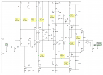
Here's the updated schematic
Here's how the overdrive protection / clamps work:
Zener diode D8 provides a starting voltage for the VAS bias such that the current is about 1mA above the target current we want. The bias action is now to engage Q15 just enough to shunt the zener into dropping bias voltage enough to reach the desired VAS current.
This change was needed so that when overdriven with a positive signal, the bias wouldn't try to pull down the bias voltage all the way leaving both legs without current and putting it into an indeterminate state. Now, however, if the VAS current reduces during overdrive, the bias shunt Q15 won't be invoked; It doesn't matter whether there's a positive or negative overdrive; the VAS current would go down as one device closes while the other opens up. The actual current is set by the closing device.
Now that the "maximum" VAS current is defined this way (target + ~1mA), this acts as protection too, and now the shunt clamps Q12/D5 and Q14/D9 will shunt excessive current from the LTP to the supplies on overdrive while preventing the VAS input from allowing too much current in the opening leg. By limiting this current, there will be current left in the closing leg still; the VAS thus will never be without current no matter how severe the input stage would be overdriven.
It works amazingly well I've did my obligatory THD 200K check and with minor tweaks to the inputstage, does 0.000% on the instrument still, that's below 0.0005%.
Is the actual schematic too hard to grasp? Is it too out of this world?
Here's how the overdrive protection / clamps work:
Zener diode D8 provides a starting voltage for the VAS bias such that the current is about 1mA above the target current we want. The bias action is now to engage Q15 just enough to shunt the zener into dropping bias voltage enough to reach the desired VAS current.
This change was needed so that when overdriven with a positive signal, the bias wouldn't try to pull down the bias voltage all the way leaving both legs without current and putting it into an indeterminate state. Now, however, if the VAS current reduces during overdrive, the bias shunt Q15 won't be invoked; It doesn't matter whether there's a positive or negative overdrive; the VAS current would go down as one device closes while the other opens up. The actual current is set by the closing device.
Now that the "maximum" VAS current is defined this way (target + ~1mA), this acts as protection too, and now the shunt clamps Q12/D5 and Q14/D9 will shunt excessive current from the LTP to the supplies on overdrive while preventing the VAS input from allowing too much current in the opening leg. By limiting this current, there will be current left in the closing leg still; the VAS thus will never be without current no matter how severe the input stage would be overdriven.
It works amazingly well
I've did my obligatory THD 200K check and with minor tweaks to the inputstage, does 0.000% on the instrument still, that's below 0.0005%.Is the actual schematic too hard to grasp? Is it too out of this world?
Attachments
Here is the basic concept of the vas. Q38,Q39 can be driven by either a diamond buffer or just conventional CFB input. In here lies the difference with your circuit. Patented by Grosser in 1991. A diamond buffer is much more linear than LTP so they didnt bother including more complexity to improve performance as they could obtain -70 db THD at 2 MHz.
I built a small 50w power amp around the circuit, works no problem although I couldnt find any benefit to what I hear compared to just a conventional CFB design with much lower complexity.
I built a small 50w power amp around the circuit, works no problem although I couldnt find any benefit to what I hear compared to just a conventional CFB design with much lower complexity.
Attachments
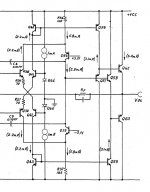
Yeah it looks similar but it's definitely different. In the VAS you show, the mirror outputs provide rails for the output bias transistors Q57 Q58 to 'glide' along as their bases are moved by Q54 and Q55's collector node, which seems to be the actual voltage output, rather than the mirror outputs are. It's a clever output stage I have to say. I'm sure the inputs of Q38 and Q39 can't be conncted - they need to have a voltage bias applied. But then again, I may be wrong in my understanding
You say a diamond buffer is more lineair contrary to an LTP. Are you suggesting the VAS you show has a diamond buffer as its inputstage, not shown?
I designed around a single LTP, contrary to a double symmetrical LTP to avoid having two control signal paths (error signals). One LTP gives me one push-pull output. This would allow the use of the 15pF compensation cap between the output and the VAS input having made it a single inverting input by tying the bases together of the VAS input devices. By implementing the signal paths this way is what made the THD figures drop dramatically. To have a push-pull VAS that has just one input. Another benefit is that I didn't need to hunt for P JFETs and try to obtain complementairy pairs having to match them.
The added complexity is mostly because of the auto bias feature I included. I wanted that to compensate for mirror errors, temperature drift and component differences. The prototype has no matched transistors, I just arbitrary grabbed them as needed
I'll have to try a diamond buffer input and see how that goes
Can you post the patent number?Patented by Grosser in 1991.
There, I made a different version without the autobias feature. I wanted to see how much it would reduce part count. I havev to admit though that at HF (100K) THD performance is worse with the bias circuit. It's not much and the performance is still miles and miles better than the fully summetrical amp I made. But without the bias circuit I was able to do 250KHz full power and still have 0.000% (> 100dB) THD. At 2MHz it was down to 76dB.
Without the bias, the VAS current will be subject to inaccuracies no more than your average run off the milll VAS. I turned the current mirrors into Wilson mirrors to ensure the mirror currents are as accurate as possible.
Attached you'll find the schematic without the bias feature. The current is now coarsely set by D8. It is equal to (5.6V - 4 x Vbe) / (R14 + R15).
This week I'll implement this current schematic on the plugboard and see if it still works as intended in reallife. But I have to order a bunch of various zener diodes; without them I can't build and test. Updates soon!
Attachments
Can you post the patent number?
Sorry gentlemen, I dont have the number. I just kept relevant schematics from the patents I deemed excellent or innovative. Its not too difficult to find though, use google patent search and search for Grosser. He has quite a few, many of AD current range of very high performance opamp designs are his doing.
Interesting about the Patent, however I seem to recall a circuit very similar to the latest version posted by MagicBox from the 1970's. without the FET input stage, which was used for a high-power Amplifier design here in the UK at that time. Might be some 'Prior Art' in this?
Interesting about the Patent, however I seem to recall a circuit very similar to the latest version posted by MagicBox from the 1970's. without the FET input stage, which was used for a high-power Amplifier design here in the UK at that time. Might be some 'Prior Art' in this?
Yeah the circuit could operate without input stage. It's just that the bases need to be bias'ed around ground. I've found though that with the additional gain of an input stage the combination (input + VAS) yields much lower distortion. It however doesn't do anything to bandwith which is limited mainly by Cmiller of the VAS output.
- Status
- This old topic is closed. If you want to reopen this topic, contact a moderator using the "Report Post" button.
- Home
- Amplifiers
- Solid State
- My New VAS Topology