Thanks for your reply.
Thinking that a higher power rating version is easier to scale 'down' rather than scaling 'up' a lower power design....
Mik
") In this design the scaling is very easy, either up or down. It's just that high power amps come with hefty demands on PSUs, need protection circuits and more, contrary to lower power designs. Cost will also increase.
In this design the scaling is very easy, either up or down. It's just that high power amps come with hefty demands on PSUs, need protection circuits and more, contrary to lower power designs. Cost will also increase.I'd like to design it such way it would be most accessible for people to build so they can enjoy their own MF series amp
My thinking is along the lines of having a single PCB design which can be populated as needed for the Power Output which the end user wants.
Mik
You mean leaving space for an additional set of output trannies for 4 or 2 ohm operation? Personally I would design for 4 ohm, 8ohm would come free
I think I'll stick with 100W/8Ohm and I will use MOSFET output stage. Someone else might want to design a suitable 3EF with BJTs and its associated bias and protection.
But that would be two different boards. I'll focus on the MOSFET design first. While I personally use the Excion parts, any lateral power FET will do.
Just as with the 3EF BJT output, someone would have to design the stage with hexfets (IRF240 etc) along with the required bias.
No matter what choice, the 3 output stage kinds each require its own PCB design.
I will take care of the lat-fet version
Now I've gotta find a distinghuisble name for this VAS. I don't have a cool last name like mr. Hawksford or Baxendall, so I'm not sure of "<last-name>-TIS" would be a good choice
Edit: I think I got it! :
SIDMO-TIS (Single-ended IN, Differentially Mirrored OUT). Sounds good or no?
Edit: I think I got it! :
SIDMO-TIS (Single-ended IN, Differentially Mirrored OUT). Sounds good or no?
Last edited:
Your output stage provides no voltage distortion to tax the VAS. Feedback applies negative distortion at the OPS input to cancel it's distortion. The VAS's job is to attenuate this distortion at it's own input. Seeing it this way you can see miller compensation is a direct leakage path of OPS voltage distortion to the VAS input.
So we don't have the final word on this VAS until you test it with a nonlinear output voltage.
So we don't have the final word on this VAS until you test it with a nonlinear output voltage.
Hi Keantoken, thanks for commenting.
Yeah you're right that the absense of a 'real' OPS doesn't tax the VAS as intended. I'm using an ideal OPS though to eliminate distortion introduced by an OPS while I would focus on developing and improving the VAS' performance itself. I'll add a real output stage later. The buffer as shown now is part of the VAS and serves to isolate the VAS output from the OPS devices. For a BJT OPS this buffer may be adapted to suit a 3EF OPS, but I'll be using the buffer as is to drive the MOSFETS I'll be using.
----
Well! Meanwhile I've succeeded in simulating the circuit in LTspice. It took a little to get accustomed to the schematic entry but figured out things quickly. The first thing I did was to add mr. Cordell's models to the LTspice library files which worked out well. The schematic uses these models for all the transistors.
Cordell's model file also contained a number of drivers, and I figured, why not try them over the MJE340/350 pairs. A quick glance across the 2SC3601 and 2SA1407 told me these were the perfect drivers to use. With them, and a small circuit adoption, THD dropped a magnitude. These guys are fast
Well, then I got into specifying the spice commands and defining parameters (thanks jxc for the .option plotwinsize=0 option) and began to get some results from the schematic. I have to say LTspice's results are very consistent, much better than Multisim. The results were very exciting! One thing LTspice proves is the consistent bandwidth and low THD associated with the topology.
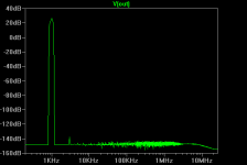
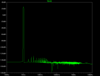
I've attached an FFT at 1KHz and 20KHz full-power, and here THD results:
20KHz Full power:
That's a lot of zeros no? It gets even better at an input signal corresponding to the first watts:
Sub-ppm performance across the full audio power band
The performance exceeds my expectations It took a little tuning it optimally but the results are there.
Now, the next thing to do is to put a real output stage in and see how much the THD will be decimated
Yeah you're right that the absense of a 'real' OPS doesn't tax the VAS as intended. I'm using an ideal OPS though to eliminate distortion introduced by an OPS while I would focus on developing and improving the VAS' performance itself. I'll add a real output stage later. The buffer as shown now is part of the VAS and serves to isolate the VAS output from the OPS devices. For a BJT OPS this buffer may be adapted to suit a 3EF OPS, but I'll be using the buffer as is to drive the MOSFETS I'll be using.
----
Well! Meanwhile I've succeeded in simulating the circuit in LTspice. It took a little to get accustomed to the schematic entry but figured out things quickly. The first thing I did was to add mr. Cordell's models to the LTspice library files which worked out well. The schematic uses these models for all the transistors.
Cordell's model file also contained a number of drivers, and I figured, why not try them over the MJE340/350 pairs. A quick glance across the 2SC3601 and 2SA1407 told me these were the perfect drivers to use. With them, and a small circuit adoption, THD dropped a magnitude. These guys are fast
Well, then I got into specifying the spice commands and defining parameters (thanks jxc for the .option plotwinsize=0 option) and began to get some results from the schematic. I have to say LTspice's results are very consistent, much better than Multisim. The results were very exciting! One thing LTspice proves is the consistent bandwidth and low THD associated with the topology.
I've attached an FFT at 1KHz and 20KHz full-power, and here THD results:
20KHz Full power:
Code:
[SIZE=2]Fourier components of V(out)[/SIZE]
[SIZE=2]DC component:-0.00779925[/SIZE]
[SIZE=2]Harmonic Frequency Fourier Normalized Phase Normalized[/SIZE]
[SIZE=2]Number [Hz] Component Component [degree] Phase [deg][/SIZE]
[SIZE=2]1 2.000e+04 3.000e+01 1.000e+00 179.80° 0.00°[/SIZE]
[SIZE=2]2 4.000e+04 4.152e-07 1.384e-08 92.73° -87.07°[/SIZE]
[SIZE=2]3 6.000e+04 9.659e-07 3.220e-08 -25.49° -205.29°[/SIZE]
[SIZE=2]4 8.000e+04 1.839e-08 6.130e-10 -11.77° -191.57°[/SIZE]
[SIZE=2]5 1.000e+05 2.775e-07 9.251e-09 132.76° -47.03°[/SIZE]
[SIZE=2]6 1.200e+05 1.355e-08 4.516e-10 -68.93° -248.73°[/SIZE]
[SIZE=2]7 1.400e+05 7.171e-08 2.390e-09 -7.52° -187.32°[/SIZE]
[SIZE=2]8 1.600e+05 2.030e-08 6.766e-10 154.40° -25.39°[/SIZE]
[SIZE=2]9 1.800e+05 3.674e-08 1.225e-09 -170.61° -350.40°[/SIZE]
[SIZE=2]10 2.000e+05 2.590e-08 8.632e-10 -33.84° -213.64°[/SIZE]
[SIZE=2]Total Harmonic Distortion: 0.000004%[/SIZE]
That's a lot of zeros no?
It gets even better at an input signal corresponding to the first watts:
Code:
[SIZE=2]N-Period=1[/SIZE]
[SIZE=2]Fourier components of V(out)[/SIZE]
[SIZE=2]DC component:-0.00779932[/SIZE]
[SIZE=2]Harmonic Frequency Fourier Normalized Phase Normalized[/SIZE]
[SIZE=2]Number [Hz] Component Component [degree] Phase [deg][/SIZE]
[SIZE=2]1 2.000e+04 3.000e+00 1.000e+00 179.80° 0.00°[/SIZE]
[SIZE=2]2 4.000e+04 7.288e-09 2.429e-09 111.91° -67.89°[/SIZE]
[SIZE=2]3 6.000e+04 6.936e-09 2.312e-09 0.01° -179.79°[/SIZE]
[SIZE=2]4 8.000e+04 1.752e-09 5.841e-10 -52.57° -232.36°[/SIZE]
[SIZE=2]5 1.000e+05 3.379e-09 1.126e-09 165.43° -14.37°[/SIZE]
[SIZE=2]6 1.200e+05 2.887e-09 9.624e-10 -114.07° -293.87°[/SIZE]
[SIZE=2]7 1.400e+05 2.566e-09 8.555e-10 -29.27° -209.07°[/SIZE]
[SIZE=2]8 1.600e+05 2.379e-09 7.931e-10 27.15° -152.65°[/SIZE]
[SIZE=2]9 1.800e+05 1.736e-09 5.787e-10 134.14° -45.65°[/SIZE]
[SIZE=2]10 2.000e+05 2.198e-09 7.327e-10 114.48° -65.32°[/SIZE]
[SIZE=2]Total Harmonic Distortion: 0.000000%[/SIZE]The performance exceeds my expectations
It took a little tuning it optimally but the results are there.Now, the next thing to do is to put a real output stage in and see how much the THD will be decimated
Attachments
To test VAS voltage leakage put a signal source between the VAS output and OPS input. Test how much load this voltage source places on the VAS. It shouldn't be any, because the VAS should reject voltage errors from the output stage.
Too many buffers is counter-productive because the combined Early effect of all those buffers becomes a significant leakage path for voltage distortion. That is why triple output stages often do worse than doubles.
Too many buffers is counter-productive because the combined Early effect of all those buffers becomes a significant leakage path for voltage distortion. That is why triple output stages often do worse than doubles.
Last edited:
Would a signal source with the same frequency as the input with an amplitude of about 2 volts do?
Yes, I may remove the 2nd follower and drive the FETs with just the first stage. With the MJE340/350s, the double follower brought an improvement even with the ideal OPS. It may no longer be helpful with these new trannies.
I still haven't been able to get Bob's MOSFET models into the LTspice library. I put them all in the .mos file, but they don't show up in spice itself. I wanted to use the K134/J49 pair to test with
I still haven't been able to get Bob's MOSFET models into the LTspice library. I put them all in the .mos file, but they don't show up in spice itself. I wanted to use the K134/J49 pair to test with
Following with big interest from the beginning and finally can contribute
1) Open Cordell-Models.txt (or whatever source you have)
2) Copy the desired model(s), e.g. the whole bunch of BJTs
3) Open the Spice Model DB, e.g. {LTSpice_DIR}/lib/cmp/standard.bjt
4) Paste the models
5) Restart LTspice
Maybe not the most elegant way, but hey, it works
BR,
Holgi
The Mfet models need to go in standard.mos.
Alternatively, to keep LTSpice from idiotically erasing or silently rewriting your models at every update, paste them directly onto the schematic, change the transistor names to them and then to get the model text off the schematic you can Rclick->justification=invisible.
You can also add the test ".inc CordellModel.txt" to the schematic, but I prefer to be able to select models the usual way.
Thanks guys..
I finally got the mosfets into the library, this time I put them before all the other models, that seemed to work though don't ask me why..
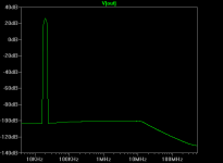
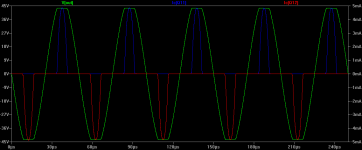
Meanwhile I made another plot of the circuit being overdriven; it shows the clipped output and the shunt currents through the IPS output clamp transistors. Does this look okay?
Later today I'll add the OPS.
I finally got the mosfets into the library, this time I put them before all the other models, that seemed to work though don't ask me why..
Meanwhile I made another plot of the circuit being overdriven; it shows the clipped output and the shunt currents through the IPS output clamp transistors. Does this look okay?
Later today I'll add the OPS.
Attachments
Thanks I'm really enjoying the development of this VAS and the thoughts behind it.
---
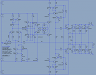
I've now added an OPS using the K134/J49 MOSFETs. I'm using 3 pairs in this configuration. The schematic as is has a gain that's good for about 100ish watts into 4Ohm.
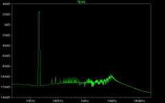
I did take out one buffer as this OPS is so slow I even had to slow down the first buffer with 100pF caps. THD is worse by 18 times with this real OPS, but it's still sub-ppm at 20K full power:
The 1KHz THD figure is still 0.000003%.
Attached a new schematic and the 1K / 20K FFTs. Oh, I also put a gain booster in the schematic, the emitter degen bypass C11 and C13. Adding this halved the THD further
Next I'll scale it up to a 250W/8Ohm / 500W 4Ohm amp and see if it still stays sub-ppm
All in all, the schematic gives a lot in return for its relative simplicity.
I'm really enjoying the development of this VAS and the thoughts behind it.---
I've now added an OPS using the K134/J49 MOSFETs. I'm using 3 pairs in this configuration. The schematic as is has a gain that's good for about 100ish watts into 4Ohm.
I did take out one buffer as this OPS is so slow I even had to slow down the first buffer with 100pF caps. THD is worse by 18 times with this real OPS, but it's still sub-ppm at 20K full power:
Code:
[SIZE=2]Fourier components of V(out)[/SIZE]
[SIZE=2]DC component:-0.00768329[/SIZE]
[SIZE=2]Harmonic Frequency Fourier Normalized Phase Normalized[/SIZE]
[SIZE=2]Number [Hz] Component Component [degree] Phase [deg][/SIZE]
[SIZE=2]1 2.000e+04 3.000e+01 1.000e+00 179.79° 0.00°[/SIZE]
[SIZE=2]2 4.000e+04 1.399e-06 4.663e-08 166.92° -12.87°[/SIZE]
[SIZE=2]3 6.000e+04 7.169e-06 2.390e-07 -61.89° -241.69°[/SIZE]
[SIZE=2]4 8.000e+04 1.417e-05 4.725e-07 -155.18° -334.97°[/SIZE]
[SIZE=2]5 1.000e+05 5.249e-06 1.750e-07 120.36° -59.43°[/SIZE]
[SIZE=2]6 1.200e+05 7.127e-06 2.376e-07 -147.68° -327.47°[/SIZE]
[SIZE=2]7 1.400e+05 2.485e-06 8.284e-08 -54.19° -233.99°[/SIZE]
[SIZE=2]8 1.600e+05 7.348e-06 2.449e-07 -140.75° -320.54°[/SIZE]
[SIZE=2]9 1.800e+05 5.006e-06 1.669e-07 -49.20° -229.00°[/SIZE]
[SIZE=2]10 2.000e+05 6.686e-06 2.229e-07 -135.21° -315.00°[/SIZE]
[SIZE=2]Total Harmonic Distortion: 0.000072%[/SIZE]Attached a new schematic and the 1K / 20K FFTs. Oh, I also put a gain booster in the schematic, the emitter degen bypass C11 and C13. Adding this halved the THD further
Next I'll scale it up to a 250W/8Ohm / 500W 4Ohm amp and see if it still stays sub-ppm
All in all, the schematic gives a lot in return for its relative simplicity.
Attachments
- Status
- This old topic is closed. If you want to reopen this topic, contact a moderator using the "Report Post" button.
- Home
- Amplifiers
- Solid State
- My New VAS Topology