Hi John
I noticed quite significant performance drop for 1622 when supply goes down to +/-2.5V. Even on light loads (inverting configuration). Would be curios to hear any insight on this.
Thank you in advance.
What output signal level were you testing at? The output voltage range is to within about 1V from the supplies. So on 2.5V supplies, you would have a max output amplitude of about 1.5Vp, or 1.06Vrms before distortion got really bad.
Definitely OK! 🙂 Anything I post on the forum I always hope other DIYers will use and improve on.
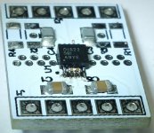
Here is one mistake not to make, below. Be sure you have specified no solder mask under the chip! I missed that one.
On mine I didn't extend the bottom heat sink foil under the SMD parts out of concern for capacitive coupling between the parts via the plane, and/or capacitive coupling from the parts to that Vee plane. The heat sink plane on the bottom looks just like the dogbone on the top. But I'm probably just over-thinking it too! I know the cap coupling [10pF max?] is very small through the 1.6mm board.
I would be curious what johnc124 thinks about the issue. Is it best to have no plane under the SMD parts, a ground plane under them, the Vee/heatsink plane, or does it even matter?
I did find an answer to that question I had a few posts back about whether removing the solder mask over the rest of the heat sink foil improves thermal transfer. I found a TI white paper on thermal pads under chips and it states that the heat transfer is about the same with or without the mask on the rest of the foil. So probably best to leave it on to prevent corrosion over time.
The big concern is going to be added parasitic capacitance at the inverting input of the op amp from the plane. The capacitance will form a pole in the loop gain curve with the feedback resistors and degrade phase margin. However, the parasitics from PCBs normally are a much bigger concern for super wideband op amps, or circuits with very large feedback resistor values. We don't really have either of those (unless your feedback resistors are 100kOhms, in which case...don't do that) so I wouldn't expect that amount of thermal plane area to cause stability troubles.
Was testing at 1Vrms. By performance drop I mean something like >20dB harmonic hight increase. Perhaps it does not fall under "really-really bad" category, but still quite noticeable.
Otherwise, quite impressed with the design! Some of my measurement results (G=-1) - http://www.diyaudio.com/forums/head...buffer-headamp-based-opa1622.html#post4703047
Also absence of input current compensation looks more as an advantage for me. It has some drawbacks.
Otherwise, quite impressed with the design! Some of my measurement results (G=-1) - http://www.diyaudio.com/forums/head...buffer-headamp-based-opa1622.html#post4703047
Also absence of input current compensation looks more as an advantage for me. It has some drawbacks.
Last edited:
Also common mode distortions seem to be well controlled. I see only 6dB rise of the second harmonic at 10kHz 2Vrms (VS=+/-10V) when I imbalance input impedances by 1k.
The third harmonic goes up more, but due to much lower initial level it remains a several dB below the 2nd.
The third harmonic goes up more, but due to much lower initial level it remains a several dB below the 2nd.
Our adaptor board is now also fully functional.
Configured in differential mode with a gain of 5.
The X7R caps will be replaced later with electrolytics.
Just for testing only.
Patrick
Configured in differential mode with a gain of 5.
The X7R caps will be replaced later with electrolytics.
Just for testing only.
Patrick
Attachments
Patrick, will your signal generator produce 200kHz, 1MHz, 3MHz square waves? If so you can compare your gain-of-plus-five amplifier's square wave response, to the square wave responses shown in post #210 for gain-of-plus-one and gain-of-minus-one.
#210 shows 1MHz and 3MHz inputs & outputs. You might decide to apply (1/5)MHz and (3/5)MHz to your PCB, or to try 1 MHz and 3 MHz directly.
edit- if the specs shown below apply to your generator, then it appears 3MHz is certainly possible. Happily, the rise time (15ns) will be less than 10% of the positive pulse (166ns) and less than 10% of the negative pulse (166ns)
_
Attachments
Last edited:
We have a 100p PPS cap on board in both +ve and feedback network.
So that is the limit in the current configuration.
In any case enough bandwidth, even with gain of 5.
Patrick
So that is the limit in the current configuration.
In any case enough bandwidth, even with gain of 5.
Patrick
How will you test for instability / unwanted oscillation? I.e. does your PCB layout minimize the bad parasitics and maximize the good ones?
We have a 100p PPS cap on board in both +ve and feedback network.
So that is the limit in the current configuration.
In any case enough bandwidth, even with gain of 5.
Patrick
I'm curious what Xen will use this for and if you will also offer boards?
//
> How will you test for instability / unwanted oscillation?
We tested the board also without the caps.
The frequency response looked essentially the same.
So you can argue that the cap does not limit the bandwidth at a gain of 5.
We are not really interested in unity gain, as we all use cross feed.
> does your PCB layout minimize the bad parasitics and maximize the good ones?
The layout has shortest possible tracks as far as 0805 resistors would allow.
So the layout is certainly not the limiting factor.
Patrick
> I'm curious what Xen will use this for .....
We were just curious.
I guess the gentleman from TI did a good advertising job.
We'll probably build a USB version using LTC3265 to generate +/-9V rails for driving 600 ohm phones from a laptop USB port, just for fun.
> and if you will also offer boards?
We have boards left, if that is the question.
But we have no time to ship one by one.
So it is better to wait until there are enough interest to do one-time multiple shipment.
PCB is 20x20mm. We cannot charge anything more than a few USD.
Paypal fees, Postage & Packing, and administrative costs will end up the major cost.
The young lady who prints address label, packs the envelopes & goes to the post office has to earn a living also.
Patrick
First sound check is good. Of course not the same as a F5-HA.
Heat sinking is necessary for low impedance phones.
The bottom surface of the adaptor board has a large pad linked to the themal pad of the chip.
It is meant to be used with a flexible thermal pad clamped between PCB and case for thermal conduction.
Patrick
Heat sinking is necessary for low impedance phones.
The bottom surface of the adaptor board has a large pad linked to the themal pad of the chip.
It is meant to be used with a flexible thermal pad clamped between PCB and case for thermal conduction.
Patrick
Last edited:
Thank you for sharing your project! I look forward to reading any thoughts you have on the sound quality of the OPA1622.
EUVL, what was missing in the one you did?
I would question those big metallic bolts. Use plastic instead and have a listen.
//
I would question those big metallic bolts. Use plastic instead and have a listen.
//
> what was missing in the one you did?
I did not. A XEN team member did.
But to answer your question :
metal case, power supply, volume pot, 3.5mm sockets, proper wiring,thermal management, maybe Class A bias, .....
> I would question those big metallic bolts.
M2 is the right size for me, as it is.
> Use plastic instead and have a listen.
No reason to use plastic as far as I am concerned.
And we already had a listen.
Patrick
OK. My suggestion was to compare metallic and plastic bolts. And build the chassis from plastic (transparent preferably due to physical properties) and you will hear proper, sat free, sound. Most boxes, other mechanics and connectors kill music, ambience and proper height.
//
//
Bypassing the OPA1622
I have received my breakout boards and started soldering.
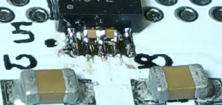
The datasheet suggests as usual to put caps as close to the chip as possible, so for fun I wanted to try if I could fit a couple 0201's right at the chip. I had some 25V 4,7nF X7R's from another project, and gave it a try.


First I soldered the chip in the reflow oven as usual, then I added a small amount of solder paste on the three legs and positioned the two caps using a needle. After a second round in the oven they now sit perfect in place. No shorts. 🙂
I am going to order a few 100nF 0201 size caps and try later.
The two next caps can then be 1uF, and the two I have under the board can be 10uF.
I will post results from measurements later.
I have received my breakout boards and started soldering.
The datasheet suggests as usual to put caps as close to the chip as possible, so for fun I wanted to try if I could fit a couple 0201's right at the chip. I had some 25V 4,7nF X7R's from another project, and gave it a try.


First I soldered the chip in the reflow oven as usual, then I added a small amount of solder paste on the three legs and positioned the two caps using a needle. After a second round in the oven they now sit perfect in place. No shorts. 🙂
I am going to order a few 100nF 0201 size caps and try later.
The two next caps can then be 1uF, and the two I have under the board can be 10uF.
I will post results from measurements later.
- Home
- Vendor's Bazaar
- New Audio Op Amp - OPA1622


