
Hi Hayk,Hello Ian.
I tried out your circuit . ... or I made a mistake in copying.
What the 5 ohm in series with the floating supplies does serve for?....
Change the bias voltage V7 to 2.29V.
V5,V6 to 1.079 as it is very sensitive.
Check T1 is 1.08mA, T2 0.76mA giving Ib T4 is 0.86mA and Ic 164mA - all at idle.
Re: 5 ohms with 10nF (R3,C1) in your circuit.
See post 13. But I moved the two RC networks and made them one, it removes the collector current drop.R15 and C6 [your R3 C1] are effectively a Zobel network that damps ringing with a triangle wave or recovery from a rail clip (something I learned from you )🙂.
Last edited:


Silly me , I have reversed the P and N drivers. First trial it doesn't work at all. I'll see it tomorrow . I also remarked , you have 10k source impedance , which should be above 100k for a VAS.
Last edited:
Ian, my models by Tins should be different than yours. Very difficultly I could make it work but good up to 3A. Never the less the result is excellent with if used in cascode . The curves are with 8 ohm and infinite source impedance. In all cases this is a switching output stage.
Attachments


Hi Hayk,
Attached is my attempt at a TINA version of my LTspice circuit. The txt suffix is necessary to accept it as an attachment. Remove it to run it.
I didn't have your TINA model for the 2SC5200 and 2SA1943. To get it to run I used standard TINA models (TIP3055 and TIP2955 with area factors of 2).
Please add you models and post it. Then I can check it against the LTspice version (and if necessary tweak it to get the TINA sim as close as possible to LTspice).
BTW I get a better derivative plot when the Gear Integration Order is set to 1 (find it in Analysis Options).
Attachments
Thank you Ian for your effort. Your output stage has three class AB biasing , the two drivers and the output. The problem one interacts with the two others, making a Chinese puzzle to adjust. I suppose The principle is to cancel the square law function of the drivers in push pull mode . What makes me hopeless , I couldn't get with any adjustment , non-switching character. I think by replacing the drivers by high performance op amp as I did , the instant I saw your circuit, is far better solution. Just an smd AD8008 and two resistors, driving NJW0281/0308, and there goes a non-switching quasi perfect crossover class AB.
2SC5200 | Bipolar Transistors / IGBTs | Toshiba Electronic Devices & Storage Corporation | Asia-English
2SA1943 | Bipolar Transistors / IGBTs | Toshiba Electronic Devices & Storage Corporation | Asia-English
Ian, you find here LT models of 2019 , I am using the Pspice model.
2SA1943 | Bipolar Transistors / IGBTs | Toshiba Electronic Devices & Storage Corporation | Asia-English
Ian, you find here LT models of 2019 , I am using the Pspice model.
Non-switching, non-switching , for what really serves to be non-switching?. In Ic/Vbe mode the base-emitter capacitors get inversely charged when it goes cut-off, which will require some time to recharge it to conduct. In Ic/Ib mode , the story is different .

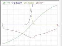
The curves above show that the transistor NJW3182 if it is maintained an idle current , instead of cut-off , 60ma (Hfe120) it has a frequency response of 100khz, but if I push it to 250ma it gets tripled . This is a dead bias current, on it comes the vivid bias via the diodes. You may be asking , 250ma idle + about 150ma vivid + 150ma driver current all this has pass through the cascode ? No, the dead currents required for proper function of the floating amplifier, can be subtracted by the supply floating current , to let pass only the vivid class A region working current.
To have minimum vivid current , I will use Shottky diodes of 0.2V . This option decreases by three fold the crossover region , that is 9 times lower power crossover region.
Attachments


Last edited:
Only-just non-switching amp in TINA
Hi Hayk,
Thanks for the links to the Toshiba models you use in TINA.
Re: What is non-switching?
As you say in Ic/Vbe mode (aka standard voltage driven mode) the base-emitter voltage reverses in standard Class-AB output stages. This creates a delayed turn on at high frequencies and hence distortion at high frequencies and it requires very fast slewing from the VAS to correct for the delayed turn on. Once a few microseconds are lost it's hard to get to where it should be since the signal is increasing rapidly. Also the VAS slew rate which drives this is limited for stability reasons, and compensation is determined primarily by the output stage HF pole. So it all depends on the output stage speed.
Now if you can prevent the base-emitter voltage reversing in standard Class-AB output stage then that goes a long way to improve the amplifiers HF linearity. The natural OPS HF distortion is lower so you don't need as much feedback to improve the HF linearity. And the secondary effect is the output stage HF pole can be consistently higher over the output swing range (assuming hard saturation is not an issue or anti-saturation methods are used).
In the new circuit attached the base-emitter voltage stays positive above +400mV so it satisfies the first primary requirement of being able to follow a fast changing input signal without the normal time delay to swing from negative to positve. The power transistor collector current does fall below 1mA at the negative output peak, which seems to make it non-switching. The primary effect is there in this circuit - namely good HF linearity. Does it matter that much if the current is not maintained at 50mA at the negative peak as long as the primary effect is there? I think I am still justified in calling it an "only just non-switching amp" as Post 84.

The attached circuit has been modified to reduce the gain of the lower half of the drivers by adding emitter degeneration.

The attached file has both the LTspice and TINA circuits using the same Toshiba 2SC5200 and 2SA1943 models. There are differences in the BC550C and BC560C Cordell and TINA models, so I have adjusted the TINA bias voltages to get the (almost) same bias and Gm (THD) plots.
I need to find a way to get the TINA BC550C and BC560C models into LTspice or vice versa (but I haven't figured out how to do that yet). Until we have the exact same BC550C and BC560C models things will still differ slightly with LTspice and TINA. But for now my TINA version is usable.
Non-switching, non-switching , for what really serves to be non-switching?. In Ic/Vbe mode the base-emitter capacitors get inversely charged when it goes cut-off, which will require some time to recharge it to conduct. ...
Hi Hayk,
Thanks for the links to the Toshiba models you use in TINA.
Re: What is non-switching?
As you say in Ic/Vbe mode (aka standard voltage driven mode) the base-emitter voltage reverses in standard Class-AB output stages. This creates a delayed turn on at high frequencies and hence distortion at high frequencies and it requires very fast slewing from the VAS to correct for the delayed turn on. Once a few microseconds are lost it's hard to get to where it should be since the signal is increasing rapidly. Also the VAS slew rate which drives this is limited for stability reasons, and compensation is determined primarily by the output stage HF pole. So it all depends on the output stage speed.
Now if you can prevent the base-emitter voltage reversing in standard Class-AB output stage then that goes a long way to improve the amplifiers HF linearity. The natural OPS HF distortion is lower so you don't need as much feedback to improve the HF linearity. And the secondary effect is the output stage HF pole can be consistently higher over the output swing range (assuming hard saturation is not an issue or anti-saturation methods are used).
In the new circuit attached the base-emitter voltage stays positive above +400mV so it satisfies the first primary requirement of being able to follow a fast changing input signal without the normal time delay to swing from negative to positve. The power transistor collector current does fall below 1mA at the negative output peak, which seems to make it non-switching. The primary effect is there in this circuit - namely good HF linearity. Does it matter that much if the current is not maintained at 50mA at the negative peak as long as the primary effect is there? I think I am still justified in calling it an "only just non-switching amp" as Post 84.
The attached circuit has been modified to reduce the gain of the lower half of the drivers by adding emitter degeneration.
The attached file has both the LTspice and TINA circuits using the same Toshiba 2SC5200 and 2SA1943 models. There are differences in the BC550C and BC560C Cordell and TINA models, so I have adjusted the TINA bias voltages to get the (almost) same bias and Gm (THD) plots.
I need to find a way to get the TINA BC550C and BC560C models into LTspice or vice versa (but I haven't figured out how to do that yet). Until we have the exact same BC550C and BC560C models things will still differ slightly with LTspice and TINA. But for now my TINA version is usable.
Last edited:

I admire you Ian how fast you could adapt to new software, it would take me months to the the same in LT.
The output stage we are dealing now is to be used as high impedance voltage follower . The VAS are mostly current sources , If you inject current instead of voltage , the 1k sense resistors doesn't operate anymore and the circuit behaves differently, unless you add a FET at the input . What is difficult to concieve in your circuit is the drivers bias, non-degenerated emitters makes very troublesome in real as is spice models are, already .
The output stage we are dealing now is to be used as high impedance voltage follower . The VAS are mostly current sources , If you inject current instead of voltage , the 1k sense resistors doesn't operate anymore and the circuit behaves differently, unless you add a FET at the input . What is difficult to concieve in your circuit is the drivers bias, non-degenerated emitters makes very troublesome in real as is spice models are, already .
Hello Ian, I tried out your circuit, with current input it doesn't work above 1A peak. Bellow yes it is excellent.
Attachments


Last edited:
Hi Hayk,
With 40uApk drive the negative side has a different input current requirement, probably due to different Beta parameters (103 for PNP vs 220).
Driving with 4mApk with 10K (below) gives the same as the previous voltage drive.

BTW I used TINA4 from 1995-2005 until LTspice appeared. TINA9 has almost the same basics but more bells and whistles.
With 40uApk drive the negative side has a different input current requirement, probably due to different Beta parameters (103 for PNP vs 220).
Driving with 4mApk with 10K (below) gives the same as the previous voltage drive.
BTW I used TINA4 from 1995-2005 until LTspice appeared. TINA9 has almost the same basics but more bells and whistles.
Attachments

Goodmorning Ian. I would like to try a pair of diamond buffers instead of push pulls in your circuit. I know there is an IC that has a pair of it probably from National Semiconductor, do you remember the reference? A quick search on TI site gave nothing.
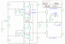
This is the 200 watt cascode version. The circuit is not yet optimized as it needs faster input error transistors . The output current being feedbacked , the frequency response and non linearity of the output Darlingtons are corrected. The idle current doesn't remain dummy at all , but if needed 20ma can be subtracted . At this stage to have a good 8A peak 10khz triangle output current , it requires a total bias idle + vivid of 275ma . Each pair of triple outputs than biased 90ma. Of course the designer can now adjust PSU voltage and numbre of cascode pairs to get lower powers.
This is extreme case ,pounding over 8A peak at 10khz, with input current of only 40ua peak.
Hayk
Attachments


Last edited:
- Home
- Amplifiers
- Solid State
- Non-switching complimentary output stage