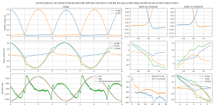
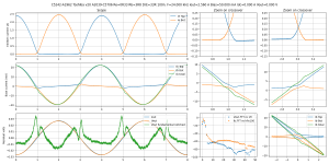
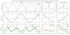
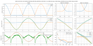
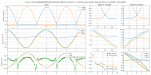
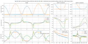
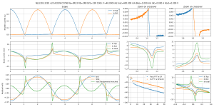
...and for comparison, the cheap C3519-A1386 clones from InChange Semi, at 1.81€ each VAT included.
Quite a big difference: while the SanKens are well matched in hFe, capacitance, turn-off, etc, the clones don't match, the PNP turns off slowly, one has a lot more capacitance than the other, and they throw in 10 extra dB high harmonics on the FFT.
Result: FAIL
Quite a big difference: while the SanKens are well matched in hFe, capacitance, turn-off, etc, the clones don't match, the PNP turns off slowly, one has a lot more capacitance than the other, and they throw in 10 extra dB high harmonics on the FFT.
Result: FAIL
Attachments
-
 scope-Bias=50.000 mA Iout=2.560 A F=48.000 kHz--C3519-A1386 ISC v20 A2039-C5706 Re=0R33 Rb=3R8 D.png292.3 KB · Views: 266
 -
 scope-Bias=50.000 mA Iout=2.560 A F=24.000 kHz--C3519-A1386 ISC v20 A2039-C5706 Re=0R33 Rb=3R8 D.png277.2 KB · Views: 268
 -
 scope-Bias=50.000 mA Iout=2.560 A F=12.000 kHz--C3519-A1386 ISC v20 A2039-C5706 Re=0R33 Rb=3R8 D.png263.2 KB · Views: 260
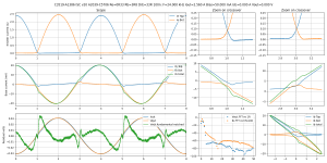
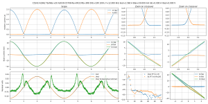
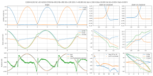
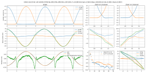
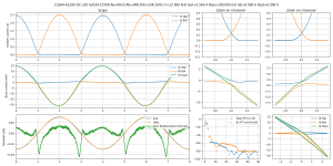
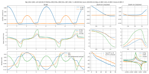
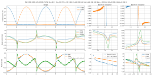
C5242-A1962 in TO3P from Toshiba...
Quite similar to the MJLs, but the MJLs give a better FFT and the smaller NJW have smaller switching spikes.
Result: meh.
Quite similar to the MJLs, but the MJLs give a better FFT and the smaller NJW have smaller switching spikes.
Result: meh.
Attachments
-
 scope-Bias=50.000 mA Iout=2.560 A F=48.000 kHz--C5242-A1962 Toshiba v20 A2039-C5706 Re=0R33 Rb=3.png287.7 KB · Views: 234
 -
 scope-Bias=50.000 mA Iout=2.560 A F=24.000 kHz--C5242-A1962 Toshiba v20 A2039-C5706 Re=0R33 Rb=3.png276.7 KB · Views: 235
 -
 scope-Bias=50.000 mA Iout=2.560 A F=12.000 kHz--C5242-A1962 Toshiba v20 A2039-C5706 Re=0R33 Rb=3.png263.2 KB · Views: 73
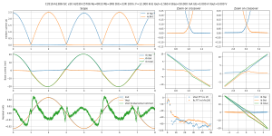
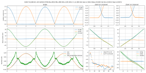
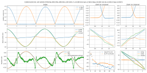
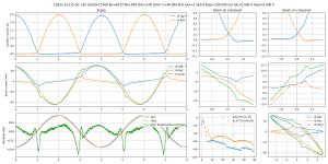
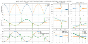
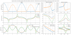
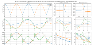
SC2837-A1186 from InChange Semi.
Unlike the previous pair from this manufacturer, these are well matched. Switching is quite soft, and capacitance is low.
Result: meh.... maybe.
Unlike the previous pair from this manufacturer, these are well matched. Switching is quite soft, and capacitance is low.
Result: meh.... maybe.
Attachments
-
 scope-Bias=50.000 mA Iout=2.560 A F=12.000 kHz--C2837-A1186 ISC v20 A2039-C5706 Re=0R33 Rb=3R8 D.png253 KB · Views: 87
 -
 scope-Bias=50.000 mA Iout=2.560 A F=24.000 kHz--C2837-A1186 ISC v20 A2039-C5706 Re=0R33 Rb=3R8 D.png263.1 KB · Views: 92
 -
 scope-Bias=50.000 mA Iout=2.560 A F=48.000 kHz--C2837-A1186 ISC v20 A2039-C5706 Re=0R33 Rb=3R8 D.png277.9 KB · Views: 88
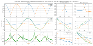
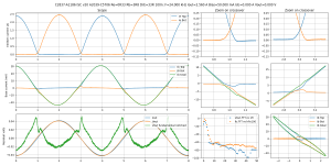
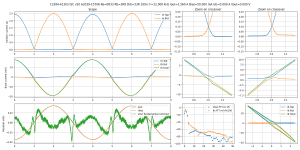
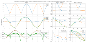
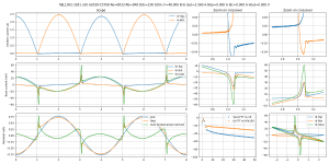
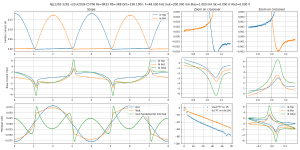
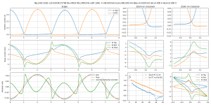
C3284-A1303 from InChange Semi.
Same story as the first pair: they don't match well, neither in switching nor in hFe, capacitance, etc.
In fact they are so similar... maybe they put the same chips in there...
Result: FAIL
Same story as the first pair: they don't match well, neither in switching nor in hFe, capacitance, etc.
In fact they are so similar... maybe they put the same chips in there...
Result: FAIL
Attachments
-
 scope-Bias=50.000 mA Iout=2.560 A F=48.000 kHz--C3284-A1303 ISC v20 A2039-C5706 Re=0R33 Rb=3R8 D.png292 KB · Views: 74
 -
 scope-Bias=50.000 mA Iout=2.560 A F=24.000 kHz--C3284-A1303 ISC v20 A2039-C5706 Re=0R33 Rb=3R8 D.png279.9 KB · Views: 73
 -
 scope-Bias=50.000 mA Iout=2.560 A F=12.000 kHz--C3284-A1303 ISC v20 A2039-C5706 Re=0R33 Rb=3R8 D.png266.6 KB · Views: 69
Last edited:
Waiting for 0 bias cases.
My next design will be 0 bias with ton of negative feedback. Investigating TMC with multiple poles. Super TMC
That was my idea long time ago.
I tried the 0 bias case but the data didn't look very useful so I skipped it to save time. But well, I have only two pairs left to test, so I added it back.
Now, clones of the legendary A1215/C2921, in the super chunky MT200 package.
hFe matching is so bad it is visible on the base current plot: one polarity is much taller than the other. Switching isn't clean either.
Result: FAIL
hFe matching is so bad it is visible on the base current plot: one polarity is much taller than the other. Switching isn't clean either.
Result: FAIL
Attachments
-
 scope-Bias=100.000 mA Iout=2.560 A F=12.000 kHz--C2921-A1215 ISC v20 A2039-C5706 Re=0R33 Rb=3R8 .png273.7 KB · Views: 92
 -
 scope-Bias=100.000 mA Iout=2.560 A F=24.000 kHz--C2921-A1215 ISC v20 A2039-C5706 Re=0R33 Rb=3R8 .png280.4 KB · Views: 105
 -
 scope-Bias=100.000 mA Iout=2.560 A F=48.000 kHz--C2921-A1215 ISC v20 A2039-C5706 Re=0R33 Rb=3R8 .png288.1 KB · Views: 117
The last pair of clones from InChange, A1295/C3264.
Results are identical to the previous one, so... probably the same chips in different packages!
FAIL
Results are identical to the previous one, so... probably the same chips in different packages!
FAIL
Attachments
-
 scope-Bias=100.000 mA Iout=2.560 A F=48.000 kHz--C3264-A1295 ISC v20 A2039-C5706 Re=0R33 Rb=3R8 .png290 KB · Views: 76
 -
 scope-Bias=100.000 mA Iout=2.560 A F=24.000 kHz--C3264-A1295 ISC v20 A2039-C5706 Re=0R33 Rb=3R8 .png278 KB · Views: 66
 -
 scope-Bias=100.000 mA Iout=2.560 A F=12.000 kHz--C3264-A1295 ISC v20 A2039-C5706 Re=0R33 Rb=3R8 .png265.9 KB · Views: 61
I tried the 0 bias case but the data didn't look very useful so I skipped it to save time. But well, I have only two pairs left to test, so I added it back.
I appreciate it.
Well, I wouldn't recommend the last two 
OK, so I did test the MJLs at zero bias, so I did another run at zero bias with C2837-A1186 because they had the most different style of switching, and that shows up nicely at 50-100mA bias.
At 0 bias... there is a difference in the size of the spikes, but there is no other detail at all.
OK, so I did test the MJLs at zero bias, so I did another run at zero bias with C2837-A1186 because they had the most different style of switching, and that shows up nicely at 50-100mA bias.
At 0 bias... there is a difference in the size of the spikes, but there is no other detail at all.
Attachments
-
 scope-Bias=0.000 A Iout=2.560 A F=24.000 kHz--MJL1302-3281 v20 A2039-C5706 Re=0R33 Rb=3R8 DrE=33.png265.3 KB · Views: 108
 -
 scope-Bias=0.000 A Iout=2.560 A F=48.000 kHz--MJL1302-3281 v20 A2039-C5706 Re=0R33 Rb=3R8 DrE=33.png275.3 KB · Views: 106
 -
 scope-Bias=0.000 A Iout=2.560 A F=24.000 kHz--C2837-A1186 ISC v20 A2039-C5706 Re=0R33 Rb=3R8 DrE.png261.2 KB · Views: 100
 -
 scope-Bias=0.000 A Iout=2.560 A F=48.000 kHz--C2837-A1186 ISC v20 A2039-C5706 Re=0R33 Rb=3R8 DrE.png281.5 KB · Views: 121
Well, I wouldn't recommend the last two
At 0 bias... there is a difference in the size of the spikes, but there is no other detail at all.
That was most beautiful graphic that I have seen regarding crossover distortion.
I don't see big dead zone though. How much feedback in dB do you have, for example at 48KHz. I don't need accurate value. Just want get the idea.
That was most beautiful graphic that I have seen regarding crossover distortion.
lmao
The graph labeled "Ib" is the base current of the output devices, not the drivers, btw. So the drivers really have to kick them through the dead zone, the base current spike is impressive!
That's with the 100MHz fT drivers. With MJE15030-15031 which have just a few MHz fT at the idle current they run at, it would be much worse.
I don't see big dead zone though. How much feedback in dB do you have, for example at 48KHz. I don't need accurate value. Just want get the idea.
No feedback, it's open loop.
There is 0.7V bias between the bases, instead of about 1.2V to turn both transistors on. That means the dead zone is about 0.5V. With 8 ohms load, that corresponds to just 62 mA. Current peak amplitude is 2.5A with 8 ohms load, so the 62mA dead zone looks really tiny.
I'll let the ThermalTraks in because tomorrow I want to test the response of the built-in diode sensor, so I'm not desoldering them now... so I've set it to run with smaller peak currents to see what happens to that dead zone.
Here's your order
0.5V dead zone, with lower current, so it's more visible.
There's a DC offset on the output because it's open loop and when both transistors are off, nothing controls the output, so the software that adjusts the output to zero... doesn't.
0.5V dead zone, with lower current, so it's more visible.
There's a DC offset on the output because it's open loop and when both transistors are off, nothing controls the output, so the software that adjusts the output to zero... doesn't.
Attachments
-
 scope-Bias=0.000 A Iout=600.000 mA F=48.000 kHz--NJL1302-3281 v20 A2039-C5706 Re=0R33 Rb=3R8 DrE.png269.5 KB · Views: 298
 -
 scope-Bias=0.000 A Iout=400.000 mA F=48.000 kHz--NJL1302-3281 v20 A2039-C5706 Re=0R33 Rb=3R8 DrE.png270.4 KB · Views: 295
 -
 scope-Bias=0.000 A Iout=200.000 mA F=48.000 kHz--NJL1302-3281 v20 A2039-C5706 Re=0R33 Rb=3R8 DrE.png270.2 KB · Views: 291
 -
 scope-Bias=0.000 A Iout=100.000 mA F=48.000 kHz--NJL1302-3281 v20 A2039-C5706 Re=0R33 Rb=3R8 DrE.png265.8 KB · Views: 301
I set bias to 1mA. It isn't very accurate because the micro has a 12 bit ADC and the gain is set for the full scale current of 2.5A, so that's basically one bit.
It's pretty nasty.
It's pretty nasty.
Attachments
-
 scope-Bias=1.000 mA Iout=100.000 mA F=48.000 kHz--NJL1302-3281 v20 A2039-C5706 Re=0R33 Rb=3R8 Dr.png286.8 KB · Views: 294
 -
 scope-Bias=1.000 mA Iout=200.000 mA F=48.000 kHz--NJL1302-3281 v20 A2039-C5706 Re=0R33 Rb=3R8 Dr.png290.6 KB · Views: 96
 -
 scope-Bias=1.000 mA Iout=400.000 mA F=48.000 kHz--NJL1302-3281 v20 A2039-C5706 Re=0R33 Rb=3R8 Dr.png284.2 KB · Views: 74
 -
 scope-Bias=1.000 mA Iout=600.000 mA F=48.000 kHz--NJL1302-3281 v20 A2039-C5706 Re=0R33 Rb=3R8 Dr.png283.6 KB · Views: 72
...and with 10mA bias.
Attachments
-
 scope-Bias=10.000 mA Iout=600.000 mA F=48.000 kHz--NJL1302-3281 v20 A2039-C5706 Re=0R33 Rb=3R8 D.png298.3 KB · Views: 77
 -
 scope-Bias=10.000 mA Iout=400.000 mA F=48.000 kHz--NJL1302-3281 v20 A2039-C5706 Re=0R33 Rb=3R8 D.png292.7 KB · Views: 92
 -
 scope-Bias=10.000 mA Iout=100.000 mA F=48.000 kHz--NJL1302-3281 v20 A2039-C5706 Re=0R33 Rb=3R8 D.png296.3 KB · Views: 94
 -
 scope-Bias=10.000 mA Iout=200.000 mA F=48.000 kHz--NJL1302-3281 v20 A2039-C5706 Re=0R33 Rb=3R8 D.png292.1 KB · Views: 80
@peufeu
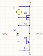
Could you consider analyzing this CPLHF output stage I have used in my last two projects? Idea is to use two well-matched same type MOSFETs in push-pull arrangement for good cancelation of gm nonlinearity. I am using it with high bias current enabling continuous class A operation. However, this arrangement seems to provide smooth transition to class AB operation, so it might be interesting also in the context of this thread.
Its important feature is that it ensures ΔVgs1 = -ΔVgs2, at least at low frequencies, both for excitation from input or output side. Source resistors are omitted for closer fit to square low (although it could be different story when used with lower bias current).
In my latest implementation Q1=IRF9610, Q2=Q3=IRFP240, Rgs=270R, I1~32mA (adjustable and thermally compensated for Vgs(t) of MOSFETs).
Attachments
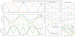
Anyway. What do all these curves say? Some of them look pretty ugly...
With the input grounded and current injected into the output, gm is 1/Zout, or d(Iout)/d(Vout). And 1/gm is just d(Vout)/d(Iout) which is the dynamic output impedance.

And, still with the input grounded...
d(Vout)/dt = d(Vout)/d(Iout) * d(Iout)/dt = 1/gm d(Iout)/dt
The portion of sinewave current near zero crossing approximates a straight line, which means dI/dt is proportional to frequency f and current peak amplitude Io, therefore
d(Vout)/dt =~ 1/gm * 2.pi.f.Io
So looking at the 1/gm curve gives us the derivative of Vout, or if the input is not grounded, the derivative of the error voltage added by the output stage which is -V(in,out) on the schematic above.
The output stage has quite a bit of base-emitter capacitance, which sits between the input and the output. In order to make this output stage push some AC current into the load, Vbe's have to move, which means this capacitance has to be charged and discharged. And, since i=C dv/dt...
In the crossover zone, base current due to B-E capacitance =~ 1/gm * capacitance * 2.pi.f.Io
Note I'm not talking about amplitude of a sinewave, but about instantaneous current.
Therefore, wiggles in gm cause a distortion in the base current which is proportional to the amplitude of the wiggles, multiplied by capacitance * 2.pi.f.Io.
These are highlighted in green on this plot:

These are not turn-off spikes due to charge storage! This is simply gm dropping a bit as one transistor passes low current, which requires Vbe to swing faster, which requires more current to charge Cbe. There are two spikes because it is biased a bit above optimal, such that the gm curve has two wiggles.
Additionally, when the transistor is off, its B-E capacitance still exists, and its Vbe moves, therefore there is an off-state base current due to capacitance. This is highlighted in blue. Off-state capacitance is proportional to the slope of the highlighted portions of the Ib curve.
Looking at the XY plot at the bottom right (X is output current and Y is base current): at low frequency, capacitance matters less, so it looks like this:

At higher frequency, base current due to hFe is still in phase with the signal, but capacitance adds a 90° phase shifted base current which "opens up" the plot and makes it look more like an ellipse instead of a straight line:

This graph says a lot of things: base current of both transistors is in blue and orange, and total base current in green.
Parts fingerpainted in blue correspond to the off-state, there is no base current proportional to output current, so it has a horizontal direction. For example, the top transistor (light blue Ib) is on in the top left side, and off in the right side.
Red arrows correspond to the on-state: there is base current proportional to output current, so it has a diagonal direction.
How "elliptical" it looks depends directly on how much 90° phase shifted base current there is in these two states.
It is different in the on-state, Cbe is bootstrapped, so it appears lower (less like an ellipse), and in the off-state where it is not bootstrapped (only a little bit by the other transistor), it appears higher (the ellipse opens up).
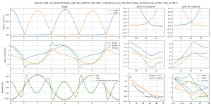
If we compare graphs at the same frequency and current peak amplitude, the base current therefore gives a good estimate of B-E capacitance. So, let's compare with 2SA1943/2SC5200 from ON, the XY plot looks completely different:

In the off-state (blue highlight) capacitance is much lower, in agreement with datasheet capacitance values.
But in the on-state (red), it appears much higher, the curve is more rounded, which means there is more 90° phase shifted capacitive current. This is not due to real capacitance, but to charge storage.
Therefore this measurement says OnSemi C5200/A1943 have less capacitance, but higher charge storage, than MJL3281/1302. For practical purposes, this means they have more apparent capacitance when they're on, and there's at least one of them on at all times, which means... the "low capacitance" feature is only looking good when the amplifier is powered off. So it looks nice in the datasheet, but "low capacitance when off" is completely useless without "low charge storage when on".
Now looking at the complete plot, this charge storage appears as extra base current at turn-off (in red on the Ib plot) which was not present in the MJL case.

Now, OnSemi C5200 and Toshiba A1943:

The top left part is the same because this is when the OnSemi C5200 is on. But the bottom right part is where the Toshiba transistor is on. Knowing that charge storage corresponds to how "rounded" the Ib curve is on this plot when the transistor is on, this says the Toshiba version has much less of it.
The Toshiba version also has lower capacitance than the MJLs. This means it looks very good, and I need a Toshiba C5200 to measure the pair. Anyone got one? RS only sells them in packs of five.
So it looks like the metric that is going to matter most for this aspect of performance is phase shift between output current and input current, which depends on the sum of capacitance and apparent capacitance due to charge storage. I will plot all the transistors on the same graph to make comparison easier (might need squinting).
With the input grounded and current injected into the output, gm is 1/Zout, or d(Iout)/d(Vout). And 1/gm is just d(Vout)/d(Iout) which is the dynamic output impedance.
And, still with the input grounded...
d(Vout)/dt = d(Vout)/d(Iout) * d(Iout)/dt = 1/gm d(Iout)/dt
The portion of sinewave current near zero crossing approximates a straight line, which means dI/dt is proportional to frequency f and current peak amplitude Io, therefore
d(Vout)/dt =~ 1/gm * 2.pi.f.Io
So looking at the 1/gm curve gives us the derivative of Vout, or if the input is not grounded, the derivative of the error voltage added by the output stage which is -V(in,out) on the schematic above.
The output stage has quite a bit of base-emitter capacitance, which sits between the input and the output. In order to make this output stage push some AC current into the load, Vbe's have to move, which means this capacitance has to be charged and discharged. And, since i=C dv/dt...
In the crossover zone, base current due to B-E capacitance =~ 1/gm * capacitance * 2.pi.f.Io
Note I'm not talking about amplitude of a sinewave, but about instantaneous current.
Therefore, wiggles in gm cause a distortion in the base current which is proportional to the amplitude of the wiggles, multiplied by capacitance * 2.pi.f.Io.
These are highlighted in green on this plot:
These are not turn-off spikes due to charge storage! This is simply gm dropping a bit as one transistor passes low current, which requires Vbe to swing faster, which requires more current to charge Cbe. There are two spikes because it is biased a bit above optimal, such that the gm curve has two wiggles.
Additionally, when the transistor is off, its B-E capacitance still exists, and its Vbe moves, therefore there is an off-state base current due to capacitance. This is highlighted in blue. Off-state capacitance is proportional to the slope of the highlighted portions of the Ib curve.
Looking at the XY plot at the bottom right (X is output current and Y is base current): at low frequency, capacitance matters less, so it looks like this:
At higher frequency, base current due to hFe is still in phase with the signal, but capacitance adds a 90° phase shifted base current which "opens up" the plot and makes it look more like an ellipse instead of a straight line:
This graph says a lot of things: base current of both transistors is in blue and orange, and total base current in green.
Parts fingerpainted in blue correspond to the off-state, there is no base current proportional to output current, so it has a horizontal direction. For example, the top transistor (light blue Ib) is on in the top left side, and off in the right side.
Red arrows correspond to the on-state: there is base current proportional to output current, so it has a diagonal direction.
How "elliptical" it looks depends directly on how much 90° phase shifted base current there is in these two states.
It is different in the on-state, Cbe is bootstrapped, so it appears lower (less like an ellipse), and in the off-state where it is not bootstrapped (only a little bit by the other transistor), it appears higher (the ellipse opens up).
If we compare graphs at the same frequency and current peak amplitude, the base current therefore gives a good estimate of B-E capacitance. So, let's compare with 2SA1943/2SC5200 from ON, the XY plot looks completely different:
In the off-state (blue highlight) capacitance is much lower, in agreement with datasheet capacitance values.
But in the on-state (red), it appears much higher, the curve is more rounded, which means there is more 90° phase shifted capacitive current. This is not due to real capacitance, but to charge storage.
Therefore this measurement says OnSemi C5200/A1943 have less capacitance, but higher charge storage, than MJL3281/1302. For practical purposes, this means they have more apparent capacitance when they're on, and there's at least one of them on at all times, which means... the "low capacitance" feature is only looking good when the amplifier is powered off. So it looks nice in the datasheet, but "low capacitance when off" is completely useless without "low charge storage when on".
Now looking at the complete plot, this charge storage appears as extra base current at turn-off (in red on the Ib plot) which was not present in the MJL case.
Now, OnSemi C5200 and Toshiba A1943:
The top left part is the same because this is when the OnSemi C5200 is on. But the bottom right part is where the Toshiba transistor is on. Knowing that charge storage corresponds to how "rounded" the Ib curve is on this plot when the transistor is on, this says the Toshiba version has much less of it.
The Toshiba version also has lower capacitance than the MJLs. This means it looks very good, and I need a Toshiba C5200 to measure the pair. Anyone got one? RS only sells them in packs of five.
So it looks like the metric that is going to matter most for this aspect of performance is phase shift between output current and input current, which depends on the sum of capacitance and apparent capacitance due to charge storage. I will plot all the transistors on the same graph to make comparison easier (might need squinting).
This is all the base currents of all the NPNs on 48kHz.
Of course the plot is unreadable, but that is not the point: notice the 2 vertical lines at +1A and -1A output current. The more off-state capacitance (or on-state charge storage) the longer they are. Therefore, I chose the length of these lines for each transistor as a metric.

This provides a nice convenient number, both for off-state capacitance and charge storage. It has no particular units, although it could probably be converted to picofarads with some math but... who cares.

In terms of charge storage, ie on-state apparent capacitance:
First place: Bensen's SanKens
Second place: MJLs, NJL, NJW family
In terms of pure capacitance:
C2837-A1186 from InChange Semi
Interestingly, charge storage and off-state B-E capacitance appear to be inversely related.
This means I can test for the effects of both by using only two transistor pairs, at the opposite ends of this "spectrum". That should save time.
With emitter resistors, both off-state capacitance and charge storage cause problems.
In a resistor-free output stage, the off-state BE capacitance is bootstrapped a lot better by the other transistor, because there is no current-dependent voltage drop across the resistors, and gm is much higher. So, capacitance is less of a problem. But there is no circuit-based cure for charge storage, it depends on semiconductor secret sauce. Even with a non-switching topology, charge storage will still manifest as an increase in capacitance when the transistor is on, it is not just a turn-off problem.
Of course the plot is unreadable, but that is not the point: notice the 2 vertical lines at +1A and -1A output current. The more off-state capacitance (or on-state charge storage) the longer they are. Therefore, I chose the length of these lines for each transistor as a metric.
This provides a nice convenient number, both for off-state capacitance and charge storage. It has no particular units, although it could probably be converted to picofarads with some math but... who cares.
In terms of charge storage, ie on-state apparent capacitance:
First place: Bensen's SanKens
Second place: MJLs, NJL, NJW family
In terms of pure capacitance:
C2837-A1186 from InChange Semi
Interestingly, charge storage and off-state B-E capacitance appear to be inversely related.
This means I can test for the effects of both by using only two transistor pairs, at the opposite ends of this "spectrum". That should save time.
With emitter resistors, both off-state capacitance and charge storage cause problems.
In a resistor-free output stage, the off-state BE capacitance is bootstrapped a lot better by the other transistor, because there is no current-dependent voltage drop across the resistors, and gm is much higher. So, capacitance is less of a problem. But there is no circuit-based cure for charge storage, it depends on semiconductor secret sauce. Even with a non-switching topology, charge storage will still manifest as an increase in capacitance when the transistor is on, it is not just a turn-off problem.
Last edited:
The good old 2N2369A transistor was built on a specialized semiconductor fabrication process which minimized charge storage. I believe its junctions were doped with gold (!) which apparently did the trick. But it was a low voltage (12V) device intended for saturated switching in digital logic. Lots of first generation supercomputers used it, most notably the CDC-6600.
Maybe you could decap a TO-3 device, load it into an ion implanter machine, and blast in some gold atoms? Probably need to do a couple dozen parts to schmeer across a range of implanter settings.
Maybe you could decap a TO-3 device, load it into an ion implanter machine, and blast in some gold atoms? Probably need to do a couple dozen parts to schmeer across a range of implanter settings.
- Home
- Amplifiers
- Solid State
- Power amp OUTPUT STAGE measurements shootout