In pcm2dsd for 44k1 and 48k there's the same code. So if it works for 48k, it must work for 44k1...I had some issues running the "latest" pcm2dsd firmware as it did not work properly for 44k1 sample rate (or multiples). I need to check that further.
This may be a timing issue between MCU and FPGA so not necessarily related to FPGA FW.So if it works for 48k, it must work for 44k1...
Are you doing anything to minimize stray coupling between EMI/RFI noise sources and the sensitive parts of the dac, maybe using ground planes as shields?My plan is to fit the dac, display and PSU ("SilentSwitcher") in a 160x100mm Hammond 1455 box.
That was more or less the case with Iancanada RPi stacks at one time. Nobody had specifically tested for noise coupling. One day I wanted to scope some signals and separated two boards with a 90-degree angle GPIO bus adapter so I access the bottom of one of the boards with a scope probe. Noticed the dac sounded better. That resulted in some more physical separation experiments between other boards in the stack, which further improved SQ. Sometime after that Ian was able to duplicate the experiments and then developed some shielding products that helped. Only point is nobody knew there was a problem up to that point because nobody had ever heard of any issues like that, so nobody thought there was a need to check. Of course, that was very different dac setup, and what was found there may not be applicable here. Just mentioned it because the experience raised my awareness of possible problems.
@MarcelvdG & All here: First I would like to wish you all a Merry Christmas - hope this time of year may be fine for you ")
And then I have a question probably for Marcel regarding the output stage used in his RTZ FIRDAC: As it is I keep experimenting with a NoDAC approach and with the current iteratioin observe that this kind of DAC "likes" an input impedance of the subsequent amplifier that is not too high. Thus, I am using the RTZ FIRDAC output stage for these NoDAC trials.
However, since these NoDACs themselves have output impedances that are slightly higher than the RTZ FIRDAC's I wonder if you might be able to help with a guideline as to how to calculate the correct values for the RTZ FIRDAC circuitry if the input impedance is different from the approx. 376 ohms of the FIRDAC? I have simulated some values for a NoDAC 1.5k output resistor (845 ohm=> 1.5k; 8.2nF=>2.2nF; 2.2nF=>1.5nF ... second stage: first 453 ohms => 220 ohm so that the amplification is increased) but I am not sure these are optimum values.
Any chance there is a "simple/straightforward" way to calculate the correct values considering different input impedances?
Cheers & have a fine day,
Jesper
In principle, if you want to change the filter such that it works with a different source impedance while keeping the gain the same, you can just scale all resistors in the first filter stage up and all the capacitors down by the same factor. So all resistor values in the first filter stage times four and all capacitor values divided by four, if the impedance is to increase by four. As you already noted, the capacitor at the output of the main board of the DAC is also part of the filter. The common-mode loop values need not be changed.
All in all, that's R26, R28, R31, C11, R50, R55, R62, C22, their colleagues from the other channel, and C15, C26, C42, C53 from the main DAC board.
All in all, that's R26, R28, R31, C11, R50, R55, R62, C22, their colleagues from the other channel, and C15, C26, C42, C53 from the main DAC board.
Hi Marcel - & thanks for your feedback. Hmmm ... so with a 1.5k (NoDAC) input resistor there will be a slight increase in the noise level if the amplification factor is to be maintained. Things to ponder but very good to know that scaling of the components is the way to go - thanks again!
Cheers, Jesper
Cheers, Jesper


Wondering if anything ever came of that?...I can report that it does make a difference and I believe that the difference is positive. Subtle but positive. I have not yet worked out what the acoustic differences are so I will continue to listen to both during the rest of the working days this week.
Don't understand why do it that way?This is built 'out of the box' and uses a PCM2DSD module on its input.
What you have now is pretty close to what I called the worst possible scenario:
https://www.diyaudio.com/community/...t-register-firdac.379406/page-46#post-7416497
Its so easy to make the dac sound better without changing anything on the dac itself. Galvanic isolation of USB and dual isolated +5v rails for I2SoverUSB, separate ground return wires for each isolated + and - 15v rail, and separate isolated +-15 rails for the output stage board made for a significant improvement in SQ here.
Some of those changes are shown in:
https://www.diyaudio.com/community/threads/return-to-zero-shift-register-firdac.379406/post-7417213
Hi all,
I remain inspired by Marcel's RTZ FIRDAC and thus have been considering ways to possibly/hopefully optimize the clock path to the LV574 output FFs. I have also been wondering how the output stage works ...
About the RTZ functionality:
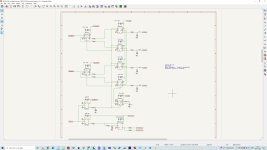
Currently with Marcel's reference design, the XOR clock doubler (U28A) signal is guided both to the output FFs (the LV574s) and to the right-most row of FFs (U22, U24, U26, U27) handling the data going to these LV574s. In an attempt to reduce the load and trace spread of the XOR clock doubler I have considered alternate approaches and have come up with the attached schematic.
It is supposed to work with e.g. something like JLSounds' USB card where the DSD_CLK is quite precise and consistent over time, i.e. situated in the middle of the DSD_DATA streams. I have also attempted to keep the DSD_DATA phase structure of Marcel's DAC.
My guess is that the attached design would work up to (and maybe higher than) DSD512, however, there might be one caveat which is the reason for this post (please note that the attached schematic screendump is a bit tiny as it couldn't be fit on my screen in a more feasible way. So I have also attached a .pdf file of the schematic).
The caveat might be the functionality of the FF handling the RTZ of the DSD DATA stream (the lower-most FF just above the XOR doubler, functional table attached). Here I use the preset & clear functionality of this lower-most LVC1G74 to clear the outputs of the DSD_DATA FFs every time the incoming DSD_CLK goes "low". That is: when the DSD_CLK goes low, _PR on the lower-most FF goes low a couple of ns later which causes a "0" on its Qnot output. This in turn "sets" a "0" on the Q outputs of all of the FFs handling the data to the LV574 output FFs. This is intended ... So far, so good.
Following this, however, the lower-most FF's _CLR is also pulled to "0" which causes both of this FF's outputs to go "high". This is also fine - maybe except for this double-"high" state not being stable. Thus, when the DSD_CLK again goes "high", according to the datasheet it will first pull _PR to "high" (this will leave Qnot on "high" as per the datasheet). When both _PR and _CLR are returned to "high" this lower-most FF is not again able to react to a clock pulse - except that both its data and clock input are grounded.
Now, the caveat to this design might be that although according to the data sheet it should work I do not know if this lower-most FF when going through this cycle may exhibit some kind of "unforeseen behavior". Might one of you know about this? Does it seem plausible that it will work?
BTW the various non-VCC capacitors are to be inserted in case adjustment of the timing is needed.
About the output stage:
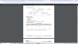
It seems to me that the time constants of the RC pairs R28/C11 & R29/C12 (3.9 ohm & 4.7 ohm and 2.2 nF) are very close to the GBW of the associated opamps (OPA2210 & -1678). I reckon this might not be accidental - but can one of you just briefly say what the benefit of this structure is? Maybe to fully cut-off opamp amplification beyond the GBW point? Might there be any "layman's name" for this amplifier structure so that I may read more about it?
Cheers & thanks for reading and maybe replying,
Jesper
I remain inspired by Marcel's RTZ FIRDAC and thus have been considering ways to possibly/hopefully optimize the clock path to the LV574 output FFs. I have also been wondering how the output stage works ...
About the RTZ functionality:
Currently with Marcel's reference design, the XOR clock doubler (U28A) signal is guided both to the output FFs (the LV574s) and to the right-most row of FFs (U22, U24, U26, U27) handling the data going to these LV574s. In an attempt to reduce the load and trace spread of the XOR clock doubler I have considered alternate approaches and have come up with the attached schematic.
It is supposed to work with e.g. something like JLSounds' USB card where the DSD_CLK is quite precise and consistent over time, i.e. situated in the middle of the DSD_DATA streams. I have also attempted to keep the DSD_DATA phase structure of Marcel's DAC.
My guess is that the attached design would work up to (and maybe higher than) DSD512, however, there might be one caveat which is the reason for this post (please note that the attached schematic screendump is a bit tiny as it couldn't be fit on my screen in a more feasible way. So I have also attached a .pdf file of the schematic).
The caveat might be the functionality of the FF handling the RTZ of the DSD DATA stream (the lower-most FF just above the XOR doubler, functional table attached). Here I use the preset & clear functionality of this lower-most LVC1G74 to clear the outputs of the DSD_DATA FFs every time the incoming DSD_CLK goes "low". That is: when the DSD_CLK goes low, _PR on the lower-most FF goes low a couple of ns later which causes a "0" on its Qnot output. This in turn "sets" a "0" on the Q outputs of all of the FFs handling the data to the LV574 output FFs. This is intended ... So far, so good.
Following this, however, the lower-most FF's _CLR is also pulled to "0" which causes both of this FF's outputs to go "high". This is also fine - maybe except for this double-"high" state not being stable. Thus, when the DSD_CLK again goes "high", according to the datasheet it will first pull _PR to "high" (this will leave Qnot on "high" as per the datasheet). When both _PR and _CLR are returned to "high" this lower-most FF is not again able to react to a clock pulse - except that both its data and clock input are grounded.
Now, the caveat to this design might be that although according to the data sheet it should work I do not know if this lower-most FF when going through this cycle may exhibit some kind of "unforeseen behavior". Might one of you know about this? Does it seem plausible that it will work?
BTW the various non-VCC capacitors are to be inserted in case adjustment of the timing is needed.
About the output stage:
It seems to me that the time constants of the RC pairs R28/C11 & R29/C12 (3.9 ohm & 4.7 ohm and 2.2 nF) are very close to the GBW of the associated opamps (OPA2210 & -1678). I reckon this might not be accidental - but can one of you just briefly say what the benefit of this structure is? Maybe to fully cut-off opamp amplification beyond the GBW point? Might there be any "layman's name" for this amplifier structure so that I may read more about it?
Cheers & thanks for reading and maybe replying,
Jesper
Attachments
About the output stage:
It seems to me that the time constants of the RC pairs R28/C11 & R29/C12 (3.9 ohm & 4.7 ohm and 2.2 nF) are very close to the GBW of the associated opamps (OPA2210 & -1678). I reckon this might not be accidental - but can one of you just briefly say what the benefit of this structure is? Maybe to fully cut-off opamp amplification beyond the GBW point? Might there be any "layman's name" for this amplifier structure so that I may read more about it?
It's a trick to compensate for the extra phase shift due to the finite gain-bandwidth product of the op-amp. I doubt if it is really needed, but it is cheap to implement, so I just implemented it. See section 2 of the attachment for details. I'll get back to you about the rest.
Attachments
Good morning from a pristinely frozen Denmark - beautiful in its glittery whiteness but also teeth chatteringly cold 
@bohrok2610 : Thanks for the tip - I was unaware of that, will consider it.
@MarcelvdG: Thank you also for your feedback and the attachment (which I suppose I may have missed somewhere earlier in the thread?). I shall be pleased to read into it, thanks! And about the rest of my post I am mainly trying to make sure things will work as intended so if you think the lower-most FF will work as I have described I'd appreciate just a brief comment confirming this.
Have a fine day both of you,
Jesper
- Home
- Source & Line
- Digital Line Level
- Return-to-zero shift register FIRDAC