
My intention is not for an exact mirror. I just want to keep the output SIT at the back of the chassis and the Mosfet at the front. Because the opt0coupler cannot be mirrored, there will be differences.
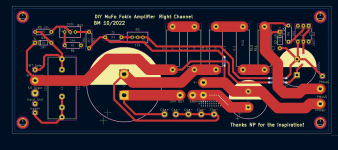
Meanwhile here is the latest right channel, with correction and tweaks:
Meanwhile here is the latest right channel, with correction and tweaks:
Attachments
If it works I'll make them available.
Since this is my first go at designing a printed circuit board, I will have to be sure that whatever I produce not only looks correct but also can be manufactured. I now have the other channel done. I still have to double check the circuit to make sure that it is correct electronically, check the footprints for size, have another overall look at them and make sure that I am happy with them, and then produce some Gerber files that hopefully will be acceptable to manufacturers.
If all goes well, I will end up with some boards that that I can test.
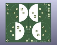
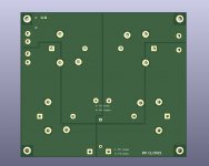
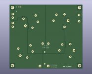
After much reviewing and tweaking here are the left and right channel boards that I am reasonably happy with.
Editing in KiCad was a learning experience. KiCad assigns Net names to component leads and PCB tracks, which are used by KiCad's "Rule Checkers" to check for conformity between schematic and PCB. Initially I was totally clueless, and that resulted in lots of error messages when running the program's "Design Rules Checker". Even more frustrating was trying to connect a track to a component lead but was sometimes prevented by the program to do so. All this was due to Net names of component leads being changed by the program during editing. But once I figured all that out, I was able to correct the Net names and editing went smoother.
So the board design is done for now and if I am still happy with them in a few days, I will probably send one board out for manufacturing. If that works out and tests ok, then the other channel will be sent out.
Attachments
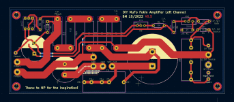
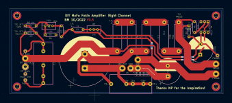
I looked at other PCBs and pondered that, but I decided to go down a different path. Everything is on the front except for locations where there are conductors crossing. The back is a ground plane.
The high current traces are 5mm wide. The maximum steady state current will be 3A. According to the KiCad calculator a 5mm x 0.035mm external layer trace can carry 3A over a distance of 150mm at a temperature rise of 1.2 degrees C, resistance of 0.015 Ohm, and voltage drop of 0.045V. For a 10 degrees C temperature rise, the current capability is 7.7A.
The board is 150mm long but the longest 5mm trace is about 100mm long. Based on these numbers I figured one side was adequate.
This is my first PCB design, and I had no previous knowledge of PCB design. I had built a few amplifier boards with Veroboard/strip board that had performed well so that experience guided me in the board layout. I tried to keep the high current paths close together and also to keep the loop areas small.
Yeah, I would think the 5mm would be fine. I only ask because-in the latest Kicad release-they made it a little easier to duplicate tracks on both layers. Kicad is more and more fun as you continue learning it’s features, or at least that’s been my experience.
One other reminder - when you go to generate the gerbers, don’t forget to generate the drill files too. I made that mistake once")
One other reminder - when you go to generate the gerbers, don’t forget to generate the drill files too. I made that mistake once
Yes, I have enjoyed using KiCad. It has been a challenge at times but it's been a good brain exercise. I also enjoy playing with LTSpice. These are great tools for diyers. Electronics diy has come a long way since I first started doing diy, when the only information available was in a few electronics magazines and textbooks.
I would also be interested in a group buy once you have it worked out.Yes, I have enjoyed using KiCad. It has been a challenge at times but it's been a good brain exercise. I also enjoy playing with LTSpice. These are great tools for diyers. Electronics diy has come a long way since I first started doing diy, when the only information available was in a few electronics magazines and textbooks.
First off...
Thank You for your hard work and willingness to share.
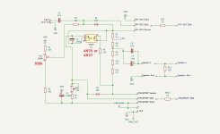
Could you clarify the value shown for C4 (Shown as 10M) ? Is this an LtSpice representation of a group of components ?
I am bouncing between a number of the SIT posts and just now starting to collect some of the harder to get and KEY items.
Thanks Again
Thank You for your hard work and willingness to share.
Could you clarify the value shown for C4 (Shown as 10M) ? Is this an LtSpice representation of a group of components ?
I am bouncing between a number of the SIT posts and just now starting to collect some of the harder to get and KEY items.
Thanks Again
milli, micro, nano, pico, femto, atto, zepto, yocto
0.001 to 0.000,000,000,000,000,000,000,001
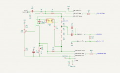
Since some are planning on collecting parts, I tweaked the schematic a bit. The 4N27 optocoupler shown in the schematic was what was available in LTSpice. In my existing strip board build, a 4N35 was used. I forgot to input the 4N35 into the KiCad schematic. The existing build has a 200k trimmer in the bias circuit and it works fine but I have decided to decreased it to 100k for a bit more current.
Meanwhile I ordered both boards from JLCPCB earlier this week and they are done and ready to ship. I opted for cheap and slow shipping as I didn't want to deal with courier customs clearing. So I expect to receive them in two to three weeks. Hopefully they will work.
I just put the existing build back into the system and I am listening to it right now - sounding good.
Here is the tweaked schematic:
0.001 to 0.000,000,000,000,000,000,000,001
Since some are planning on collecting parts, I tweaked the schematic a bit. The 4N27 optocoupler shown in the schematic was what was available in LTSpice. In my existing strip board build, a 4N35 was used. I forgot to input the 4N35 into the KiCad schematic. The existing build has a 200k trimmer in the bias circuit and it works fine but I have decided to decreased it to 100k for a bit more current.
Meanwhile I ordered both boards from JLCPCB earlier this week and they are done and ready to ship. I opted for cheap and slow shipping as I didn't want to deal with courier customs clearing. So I expect to receive them in two to three weeks. Hopefully they will work.
I just put the existing build back into the system and I am listening to it right now - sounding good.
Here is the tweaked schematic:
Attachments
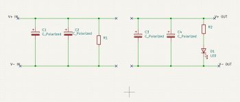
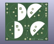
While waiting for the pcbs I played with KiCad and came up with a power supply board that will accomodate 80VDC, 5-pin 50mm diameter electrolytic capacitors. The power supply for this amplifier supplies V- but I made the board user friendly, so that it can either supply V- or V+, with a connection for a choke in the negative or positive rail. There are locations for a bleed resistor and a LED and voltage dropping resistor. The board is 125mm x 110mm in size.
My power supply for this amplifier is CLC, 2x22mF - Hammond 159ZJ - 2x22mF. Power transformer is 50VDC. I suggest 400VA minimum although I went overboard and went with 600VA. I don't know why I did that, but that was done over three years ago when I first built the amplifier as a 50W BAF2105 with THF-51S.
I won't be re-building the power supply with this new board, but I will order some test copies to make sure that it works. It was a fun exercise as I had to create the capacitor footprint; I could not find the footprint in KiCad.
Attachments
In the 1960, my father thought a One Farad Capacitor was a fine joke. Tell the new engineer to go borrow a One Farad Capacitor. Everybody in the building knew the prank, so said "Sorry! Just ran out!" or "Try the stockroom" or "Try Hank on the 10th floor!"10 MegaFarads would be a lot of fun.
He said it would be the size of a garbage can.
40 years later the boom-cars had 1F caps to carry the boom-boom load, size of a large soup can.
8 years ago I was playing with the idea of a 40F bypass cap. (Start-up time was long...........)
Wake me up when we get MegaFarads at mail-order prices. (What is this "mail order"??)
- Home
- Amplifiers
- Pass Labs
- Single Ended Tokin SIT THF-51S Common Drain Mu Follower Amplifier, 45W?