Since I've to order pcb anyway, I've started a smd version on the board.
It's a somewhat simplified version, without the sync parts and with only one irfi4212. The smd parts are all 1206 to keep things easy to solder. On the other hand, the gain stage is now onboard, with the balanced receiver but without the limiter.
Considering that ChocoHolic has a lot more experience with class-D amps than I have, the layout is heavily inspired by his (not to say an outright copy).
I'd have quite a few questions with parts replacement but I'd rather first have ChocoHolic's point of view if it'd better be done in another thread.")
It's a somewhat simplified version, without the sync parts and with only one irfi4212. The smd parts are all 1206 to keep things easy to solder. On the other hand, the gain stage is now onboard, with the balanced receiver but without the limiter.
Considering that ChocoHolic has a lot more experience with class-D amps than I have, the layout is heavily inspired by his (not to say an outright copy).
I'd have quite a few questions with parts replacement but I'd rather first have ChocoHolic's point of view if it'd better be done in another thread.
Attachments
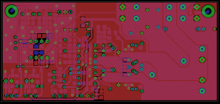
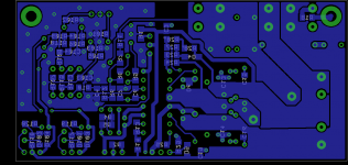
I continued working on the smd board.
Substitutions:
- all resistors go to 1206. Two exceptions, the feedback resistor and r28 (0.5w in the bom) which are both split into two 1206. And the 3w zobel of course.
- C2, C5, C4, C7 go to PPS smd caps (pana echu).
- C6 go to a 1206 np0 cap.
- most zeners and diodes go to mini-melf package.
- some decoupling caps go to 0805 package for closer decoupling.
Stuff I'm not sure about:
- C1 (the cap in // with the feedback resistors). It's a 47p FKP2 as it is. I haven't found a good substitute in smd. Not a big deal though, nothing much to be gained for going smaller.
- r30-r36, r31-r37. Having two resistors makes the layout easier. But wouldn't a jumper + a 22r resistor be better to populate the board ?
As it is, the space gain goes to two regs and a differential gain stage. I only reduced the board from 5cm to 4.7cm, to allow it to better fit on a 50mm wide, 3mm thick aluminium L.
There's still some space; I might try to fit the limiter back in.
As a side note, I tried first to get into kicad... couldn't get used to it, went back to copy the whole stuff into eagle.
Attachments
Keeping fingers crossed that you manage to solder them without damage.- C2, C5, C4, C7 go to PPS smd caps (pana echu).
Personally I cannot - at least not without causing them to drop a good portion of their capacitance or completely open.
Two more points:
1) Did you check your distances on the PCB regarding the concerned voltages?
My personal rule of thumb: Keep distances in a way that the expected peak voltages do not cause electrical fields above 300Vp/mm.
Note: This rule is intended to allow trouble free operation in normal indoor home applications. It does not serve the requirements for isolation paths which have to meet safety standards for basic or double/reinforced isolation. Fortunately the LiteAmp PCB has no such paths, it is intended to be operated from safely isolated and fused supplies.
2) For your version with just one IRFI you can also choose a 15uH choke with just half of the current rating. ==>Smaller size.
Last edited:
To me it's perfectly fine to have your version of the LiteAmp in my thread.... I'd rather first have ChocoHolic's point of view if it'd better be done in another thread.
Thanks for the comments.
- for the caps, let's not tempt the devil. NP0 are available at 1nf. For the 4.7nf, I might have to go back to through hole. The fks2 are twice as small as the fkp2, would you advice against ?
- wrt isolation. Worst case is 80v with +-40v rails. 300v per mm, that's about 300v per 40 mil. Roughly 10mil for 80v. The clearance rules are set @12mil without erc warnings so that should be ok. I'll run a check @16 mil to identify weak spots. Power planes have an isolate rule at 16mil iirc. I'd have to check the gnd plane rules, I think it's 10 mil.
Is the 40v line running down the board a deliberate separation of the input and output stages' grounds ?
Yes, something like this.For the inductor.. 55 turns of .63mm wire on a t80-2 core ?
Personally I would head for 52 turns of 0.63CuL on a T80-2.
Also 50 turns will work fine, the frequency compensation is forgiving
vs minus tolerances of the choke.
Regarding PCB distances: At such small distances better add some mil for the tolerances of the PCB manufacturer. Nevertheless - I agree as long as you stay with +/-30V...+/-40V I would also not expect much issues with the 12mils you have given. Also 10 mils for GND should be fine. Vs GND no point in the circuit will have more than 45Vp difference.
With these numbers you really need to have bad luck with a poor vendor in order to get your real PCB distances reduced in a harmful way.
Multiple people are stating that NP0 measure well, but sound harsh.NP0 are available at 1nf. For the 4.7nf, I might have to go back to through hole.
I never digged into this and likely it will depend a lot on the very specific usage in the circuit. .. so I cannot give a qualified advise here.
To me the FKS2 are perfectly fine for all points where I have used the FKP2 in the LiteAmp. They are always in circuit positions where moderate resistive portions do not hurt.The fks2 are twice as small as the fkp2, would you advice against ?
..scratching my head which 40V line you are asking about...Is the 40v line running down the board a deliberate separation of the input and output stages' grounds ?
...answered too fast:Vs GND no point in the circuit will have more than 45Vp difference.
The gate drive and floating supply of the high side will happen to reach approx. 55...60Vp vs GND worst case.
One more hint:
The collector of Q3 in my circuit is connected to +40V.
However there is no 'must do' reason to do so.
In terms of circuit design the more obvious approach would be to
connect it to Vaa (similar like the collector of Q4 is connected to Vss).
My choice to connect the collector of Q3 to +40V was just linked to some intermediate layout experimentation and then I left it this way instead of checking later again whether a connection to Vaa would have become practical again.
But of course both options work fine, as long as the voltage rating of the BJT is chosen sufficiently.
Wow, thanks. Plenty of food for thought.
- about np0: I've rather good experiences using small np0 for compensation, filtering and the like in opamps circuits. So I'm not too affraid of them. Maybe my ears aren't good enough
- about the fks2/fkp2: I'll finally keep the fkp2. Not for audiophile reasons but because the fks2 are only +-10% while the fkp2 comes in +-2,5% and it's easier not to worry about matching (call me lazy).
- for the output inductor: 52 turns will be easier to wind. 55 were just possible.
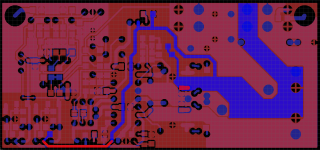
- sorry for being cryptic about the "40V line". I had in mind the two tracks in the groundplane under the irs2092, which are at +40V (they bring down the 40V line to the bottom of the board).
- a similar question about the decoupling of vaa: why bring the vias way down ?
- clearances: I've modified the board to get a clean pass at 16mils (except the groundplane, I'm getting too many cuts into it by increasing the clearance). That should account for manufacturing lack of precision.
- about q3: done, it actually simplifies routing a little bit.
It goes without saying that I'll make the eagle files freely available in the end.
- about np0: I've rather good experiences using small np0 for compensation, filtering and the like in opamps circuits. So I'm not too affraid of them. Maybe my ears aren't good enough
- about the fks2/fkp2: I'll finally keep the fkp2. Not for audiophile reasons but because the fks2 are only +-10% while the fkp2 comes in +-2,5% and it's easier not to worry about matching (call me lazy).
- for the output inductor: 52 turns will be easier to wind. 55 were just possible.
- sorry for being cryptic about the "40V line". I had in mind the two tracks in the groundplane under the irs2092, which are at +40V (they bring down the 40V line to the bottom of the board).
- a similar question about the decoupling of vaa: why bring the vias way down ?
- clearances: I've modified the board to get a clean pass at 16mils (except the groundplane, I'm getting too many cuts into it by increasing the clearance). That should account for manufacturing lack of precision.
- about q3: done, it actually simplifies routing a little bit.
It goes without saying that I'll make the eagle files freely available in the end.
- sorry for being cryptic about the "40V line". I had in mind the two tracks in the groundplane under the irs2092, which are at +40V (they bring down the 40V line to the bottom of the board).
- a similar question about the decoupling of vaa: why bring the vias way down ?
The GND concept of the LiteAmp is to have a closed GND without intensional cuts. The separation of small signals vs high current paths is solved by the position of the components and where they are connected to the GND plane. DC will simply distribute according DC resistance. For HF you have to consider a little bit of field theory in order to predict the current distributions in the GND plane. In simple words the HF current in the GND plane will always concentrate there where you are routing back the related loop on the top side. This results in the smallest loop causing the smallest inductance which dominates the total impedance at HF and consequently this is the path where the current can run most easily. There you will find the maximum of the current density distribution.
The 40V line below the IRS2092 is placed there, because I did not find a proper path on top, so I picked a position on the GNDside where it does not cut through main current paths. Please note that even below the IRS2092 I have routed it partially back on the top side in order to allow at least a mostly closed GND plane.
The decoupling of Vaa and Vss should be close and without large loop to the GND connection of the IRS2092. Obviously from this perspective the position of both caps is not perfect, but with the at least mostly closed GND plane (as described above) it is easily good enough and overall it was the most compact trade off which I found.
That clears things up; thx. I fully agree on the clean gnd plane approach.
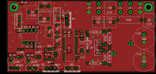
If I put the smd decoupling caps on top, in the middle of the socket, I can manage to save most of the gnd plane there. I was just hesitant to do so in case the cuts were intentional.
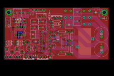
It gives something like the attached. The +40v is highlighted.
Now time to see if anything is gained by reducing the output stage's coil.
If I put the smd decoupling caps on top, in the middle of the socket, I can manage to save most of the gnd plane there. I was just hesitant to do so in case the cuts were intentional.
It gives something like the attached. The +40v is highlighted.
Now time to see if anything is gained by reducing the output stage's coil.
Attachments
I'm affraid I've still some questions. 
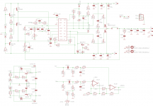
It's about the regulators used on the gainboard. What are the diodes d103-d104 for ? Protection ? But there isn't much capacitance at the output ?
And what about r112-113 ? They seem to raise the supply impedance quite a bit. Are they there to prevent oscillation of q1, q2 ?
Thanks for any pointers.
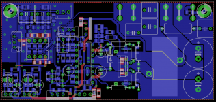
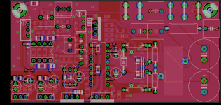
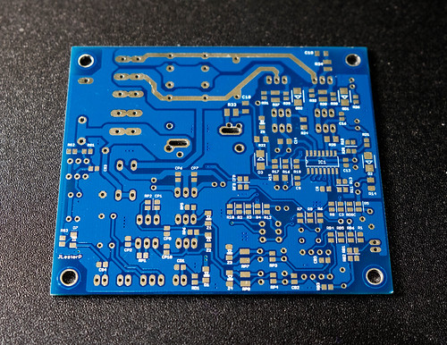
Things are slowly taking shape pcb wise.
It's about the regulators used on the gainboard. What are the diodes d103-d104 for ? Protection ? But there isn't much capacitance at the output ?
And what about r112-113 ? They seem to raise the supply impedance quite a bit. Are they there to prevent oscillation of q1, q2 ?
Thanks for any pointers.
Things are slowly taking shape pcb wise.
Attachments
Yes, D103 & 104 are for protection. Not only because of the capacitances - and I agree, most likely the small capacitances would not cause much harm.What are the diodes d103-d104 for ? Protection ? But there isn't much capacitance at the output ?
Moreover they are part of a protection, which needs the D105, 106, 107, 108 (which you already kicked out
 ).
).D105, 106, 107, 108 in conjunction with D103 and D104 and R110 & R111 and R115 & R116 are protecting the OP amp input against large input signals, even when the amp is not powered. Weakest parts of this protection with components and values as chosen in the Lite Amp are R110 & R111. The chosen values are sufficient to protect against miswiring where someone would accidentially have wired a speaker signal from another amp to this input (for amps with supply rails up to +/-40V).
R112 and R113 and also the base drive impedance ensure a short term overload protection of the internal supply. I.e. when you measure the supply but accidentially make a short with your tips. Well, with most BJTs the base drive impedance and current gain would do the job. However when you accidentially have a BJT with very high current gain, then things turn less reliable without R112 & 113.And what about r112-113 ?
In the same way like R112 & 113 are reducing the short circuit current they also narrow the spread of the output impedance of this supply.
Enlightening as usual. Thank you.
Yes, I dropped the input protection. I agree that it is a welcome feature for PA use. But my aims are strictly limited to domestic use. I'll shift d103-104 to the bases of the transistors.
As for r112-113, since the whole thing is on the pcb, I'm less concerned about shorting. I'll keep them out.
Yes, I dropped the input protection. I agree that it is a welcome feature for PA use. But my aims are strictly limited to domestic use. I'll shift d103-104 to the bases of the transistors.
As for r112-113, since the whole thing is on the pcb, I'm less concerned about shorting. I'll keep them out.
D
Deleted member 148505
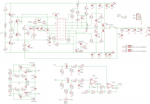
I'm also creating an implementation of the liteamp but without the differential input, and without deriving the VAA/VSS/VCC supply from the rail supply.
It also has nFatal header, so it can take advantage of SMPS's protection circuits.
For the spirit of openness, (but with limitations) I'll give (only) the gerber file once I have the measurements (may take months from now).
Special thanks to Chocoholic for giving us a high performance IRS2092 implementation.
Hi jlester87,
it is really nice to see more and more designs which got inspiration from the LiteAmp.
Some comments on your approach:
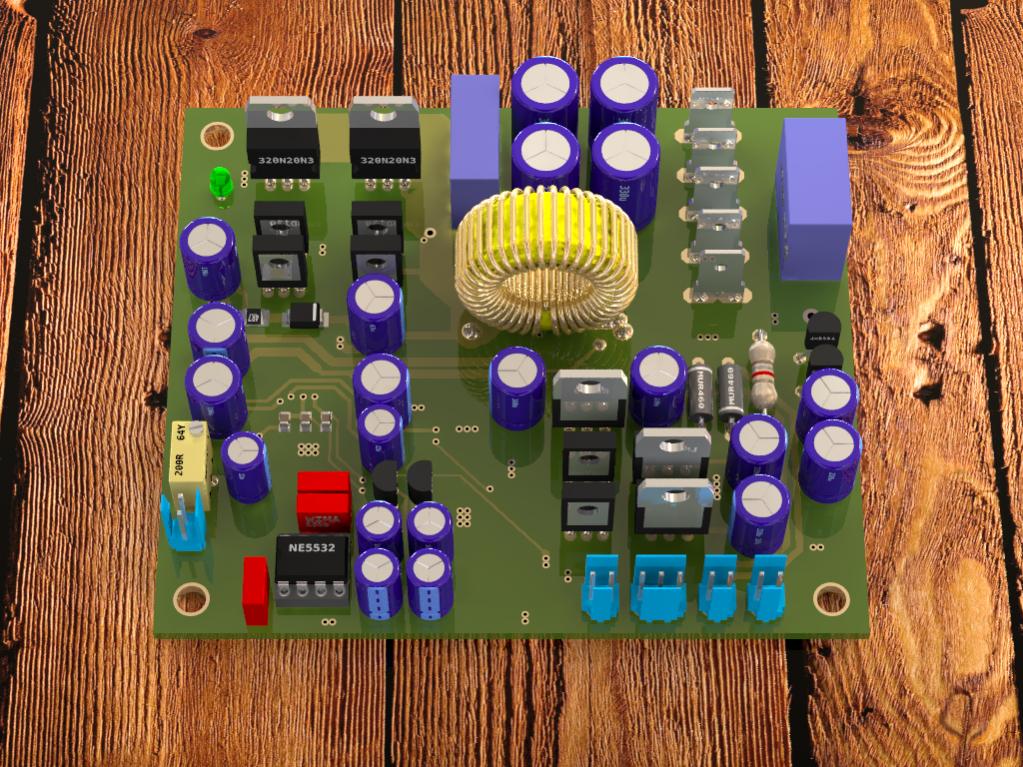
1. Stronger halfbridge based on IPD320N20N3 with BJT gate drivers.
Basically nothing wrong with this. Details you will have to adjust like in every new power stage design.
2. Arrangement / layout of half bridge & simplified rail caps:
Theoretically it will lead to more HF-ringings (20MHz..100MHz), especially in hard switching load situations. If this ringing becomes too much, you may not just see this in EMI measurements, but it can also cause undesired early tripping of the over current protection of the IRS2092. However if you already have good experience with arrangements like yours for the IRS2092, then trust on your experience.
3. You skipped R38 and C23, which I used for THD optimization for increasing the stability of the amp.
THD optimization would not match to your new half bridge anyhow and it is just a minor trimming, so don't bother about this.
Regarding stability: If you kept the output filter and global feedback and small signal area identical like in my 80V BOM, then the amp is still basically stable without R38 & C23. However the margin to handle extrem situations like load dump or start up without load becomes less. If your amp shows issues in such situations, you should have a closer look to this change.

Choco
it is really nice to see more and more designs which got inspiration from the LiteAmp.
Some comments on your approach:
1. Stronger halfbridge based on IPD320N20N3 with BJT gate drivers.
Basically nothing wrong with this. Details you will have to adjust like in every new power stage design.
2. Arrangement / layout of half bridge & simplified rail caps:
Theoretically it will lead to more HF-ringings (20MHz..100MHz), especially in hard switching load situations. If this ringing becomes too much, you may not just see this in EMI measurements, but it can also cause undesired early tripping of the over current protection of the IRS2092. However if you already have good experience with arrangements like yours for the IRS2092, then trust on your experience.
3. You skipped R38 and C23, which I used for THD optimization for increasing the stability of the amp.
THD optimization would not match to your new half bridge anyhow and it is just a minor trimming, so don't bother about this.
Regarding stability: If you kept the output filter and global feedback and small signal area identical like in my 80V BOM, then the amp is still basically stable without R38 & C23. However the margin to handle extrem situations like load dump or start up without load becomes less. If your amp shows issues in such situations, you should have a closer look to this change.
Choco
2. Arrangement / layout of half bridge & simplified rail caps.....
Now I found the small ceramic caps from the rails to GND right at the MosFets - did not see them first. Also found the snubbers (C15,R34,C16,R35).
Ok, with both in place I think your design has a good chance to work without HF resonance headache.
Component stress could become an issue. I saw just 2x1 ceramic from the rails, which is brave for your target power in PA usage.
Note, I have put 2x4 of them already for lower power.
Also the size of your R34 & R35 appears small (here heat happens under all load conditions).
D
Deleted member 148505
Hi jlester87,
it is really nice to see more and more designs which got inspiration from the LiteAmp.
Some comments on your approach:
1. Stronger halfbridge based on IPD320N20N3 with BJT gate drivers.
Basically nothing wrong with this. Details you will have to adjust like in every new power stage design.
2. Arrangement / layout of half bridge & simplified rail caps:
Theoretically it will lead to more HF-ringings (20MHz..100MHz), especially in hard switching load situations. If this ringing becomes too much, you may not just see this in EMI measurements, but it can also cause undesired early tripping of the over current protection of the IRS2092. However if you already have good experience with arrangements like yours for the IRS2092, then trust on your experience.
3. You skipped R38 and C23, which I used for THD optimization for increasing the stability of the amp.
THD optimization would not match to your new half bridge anyhow and it is just a minor trimming, so don't bother about this.
Regarding stability: If you kept the output filter and global feedback and small signal area identical like in my 80V BOM, then the amp is still basically stable without R38 & C23. However the margin to handle extrem situations like load dump or start up without load becomes less. If your amp shows issues in such situations, you should have a closer look to this change.
Choco
Now I found the small ceramic caps from the rails to GND right at the MosFets - did not see them first. Also found the snubbers (C15,R34,C16,R35).
Ok, with both in place I think your design has a good chance to work without HF resonance headache.
Component stress could become an issue. I saw just 2x1 ceramic from the rails, which is brave for your target power in PA usage.
Note, I have put 2x4 of them already for lower power.
Also the size of your R34 & R35 appears small (here heat happens under all load conditions).
Thank you for your shared insights,
I was actually experimenting with this layout, bypass caps are about an inch further from the mosfets. What I can do for now is to put another rail to rail SMD cap in the exposed tracks. In all of my other layouts, bypass caps are sitting next to the mosfets' pins. Didn't experience any early tripping on those modules, I will check for HF ringing and will test for early tripping.
R38 and C23 are intended to be put on speaker terminals on the chassis as I will recommend at least 5W rating on the resistor. I don't get what load dump means. Is this connecting/disconnecting a speaker? Can you explain this further?
Although R38 is not heating up in normal occasion (even without load attached), in certain creative situations (like too lengthy single ended cables/ dangling unconnected lengthy SE cables or where there is HF noise in the input like some desktop pc sources + lengthy cables and the modules are run in stereo, and shares the same supply and has no load connected. The resistors are heating up. We don't know how would anyone will wire the amp.
--------
Also there are no ceramic caps on the mosfet pins
, they are bleeder for gate drive.. I was expecting to get 1W rated resistors for 1210 type SMDs, but I haven't found any, only 0.5W rated types, maybe i'll just put unoptimized, low dissipation snubber for the meantime.
I will create 2 stereo units for testing, ipp530n15n3 for low power and irfb4227 for high power. I will check for some instabilities and HF ringing later.
Regards,
Lester
- Home
- Amplifiers
- Class D
- SystemD LiteAmp