This brings me to the attached layout for the output stage.
Fully agree with the position of your C203.
Watch the similarity to the center tapped C13+C14 or C17+C18.
Attachments

Thanks for all the comments, it slowly makes sense to me.
I've been checking the iraudamp 7s and 7d layout. Decoupling of the mosfet is on the light side. Two 100n caps from b+ and b- to gnd and one 100nf cap from b- to b+. All those are quite far from the mosfet pins but on big power planes. They take it easy by making the rail-to-rail cap a big through hole film cap, which can jumper over the output track, even on the smd board.
They also seem to avoid thermal reliefs. To reduce inductance and minimize cuts in the planes I suppose ?
I quickly tried to see what happens if I move the output track to the top layer. An interesting puzzle.
Attachments


Good. I'm going to explain 2 next lessons:
1- Snubbers are good but since FETs have gentle Cds at low Vds, snubbers can benefit from a few nH of inductance, no need to place parts as close to the FETs, it can be brought to the extreme of tuning the snubbes so that they draw a current peak whose maximum value happens about the center of the voltage swing, where Cds(low) in parallel with Cds(high) is at minimum, this has to be considered at moderate to high load, this can remove a good portion of turn-off losses from FETs, allowing higher value C and lower value R, with proper gate drive. I have used thru-hole 0.25W resistors for that purpose in high power amps. Some lenght of PCB trace does the same.
2- Decoupling capacitors are good, being gentle adding parts to tailor switching is good, but too many cuts in ground plane add inductance, reduce shielding, and worsen resonances, for example the one between low-esr electrolytics and ceramics, or the ones between the own ceramics. The solution for 2 side PCB is to use -V as the ground plane for the output stage and gate drive sections, and GND for the rest.
Fully agree on the snubbers.
Regarding GND considerations IMHO reliable judgement needs a detail examination in the EMI chamber and I think by the end of the day one will find pros and cons for both concepts. Also it will depend on the demanded frequency range. Cut outs for a pad of a 1210 component will be more headache in the multi GHz range.
Let's put some numbers on the snubbers for everyone who wants to experiment with the dirty hacked LiteAmp...
The heavy snubbers with 470pF are simple to apply without much tuning, they are more forgiving on the geometry of the snubber itself and also on the geometry of the realized implant of the IRFB4227 instead the original IRFI. But with this snubber we have to expect approx. 1W heat in the resistor at fs 300kHz. I used two small sized axial 39R/1W resistors in parallel in order to keep their temperature moderate. The snubber losses cannot be calculated from the simple anticipation that the resistor would dissipate the same energy like as stored/unstored in the cap. This rule is only valid when the rise time of the rectangle is short vs the RC time constant, which is not the case in this snubbers. So for loss calculation we have calculate with the real sloping speed of the half bridge, resulting in approx. 1W losses for each snubber.
Resonant tuned snubbers:
For this we need to know the frequency of the parasitic half bridge resonance(s). Then we can mod the RC snubber by tuning the parasitic L of its loop. We get a RLC snubber. Well, in reality we always have a RLC, but usually not making use of it.
Tuning works very well for resonances which show just one mode. For multimodal resonances you will have to design the snubber with wider bandwidth, or use multiple....
The more you throw multiple ceramic caps somewhere somehow in the rails, the more you have to expect multimodal resonances. (You see the potential contradiction between needs from component stress and taming EMI.....)
In case of the modified LiteAmp as described with IRFB4227 in the mounting positions of Q6 and Q7 the new resulting halfbridge suffers from a pretty large loop area involved and the resulting dominating resonance is approx. 50MHz (again dirty hack).
Other higher modes exist, but with much lower magnitude, so we can focus on the 50MHz.
From experience in other designs IRFB4227 can be snubbered reasonably well with approx 220pF, when using a tuned RLC snubber. For a 50MHz tuning we will need approx 45nH inductance of the snubber loop.
Geometric coupling points of the snubber: Personally I prefer to couple them directly to drain and source pins, as much as practical.
With a resistor value of 18R this smaller snubber will dissipate approx 0.26W heat.
These numbers are a starting point. You will have to experiment and measure pretty careful in order to really fit it to your build.
They take it easy by making the rail-to-rail cap a big through hole film cap...
Good.
I am not sure if this good was intended to comment the rail-to-rail cap, just copied both quotes close together in order to discuss wheter this is really fortunate.
I am seeing this often, but from my understanding it is not fortunate. With nothing but such a large film cap the loop through rail cap and MosFet involves unnecessary high L and the resulting parasitic resonance will contain high energy.
I don't want to give the impression that I intend to copy the iraudamp 7s design. I was just surprised by how they did things. IR's layout with the snubbers real close, no thermal reliefs and its lightweight decoupling makes less sense to me than what you two are explaining.
I quickly tried to see what happens if I move the output track to the top layer. An interesting puzzle.
Hm, this cut out already has a size which is less fortunate.
Just google 'slot antenna' or 'inverted F antenna'.
Antennas: The Inverted-F Antenna (IFA)
After reading this you will look to PCBs with different eyes 😀
Your structure most likey is suited to radiate most efficient somewhere between 1GHz...2GHz.
Oopsie. Thanks for the link.
I'm still thinking as if I was laying out a class AB amp I'm afraid.
I'm still thinking as if I was laying out a class AB amp I'm afraid.
Don't be so shy. Already your first attempt was on a level which should work without too much trouble.I'm still thinking as if I was laying out a class AB amp I'm afraid.
I'm not shy, it's just that I'm discovering stuff as I go. I really didn't consider the impact of cut-outs on radiations up till now. I'm no EE, my fields of expertise are more in law and philosophy...
More seriously, that's what makes this forum interesting; you can get insights beyond what just works.
More seriously, that's what makes this forum interesting; you can get insights beyond what just works.
IR did IRAUDAMP. Choco did SystemD. I did a highly optimized 6000W/2r LF amplifier module in icepower1000ASP size for highly demanding USA market, USA made too.
Activating testosterone with cult to aesthetics is OK for jobs not involving innovation or optimization. When a cult-to-aesthetics-guy faces an optimization/innovation problem demagogy results, as there is no way the guy can solve the problem without solving many other pending problems first. I have seen some German films where citizens with toxic or low profile personal relationships are invited to move to another country (Gegen die Wand, Ein Freund von Mir, Der Freie Wille).
Traces are like turns in a transformer. Ground plane is like a shorted turn, only where it does not have cuts. A minimum-cut layout can always be derived.
Last edited:
I'm a bit lost as to whom that last post was addressed. And quite a bit puzzled about what it means.
If it was addressed to me, there's no need to defend your credentials. As for the rest... I don't care much about aesthetics. Comparing layout is just a way to understand why people did things the way they did.
If it was addressed to me, there's no need to defend your credentials. As for the rest... I don't care much about aesthetics. Comparing layout is just a way to understand why people did things the way they did.
I'm a bit lost as to whom that last post was addressed. And quite a bit puzzled about what it means.
..same with me.
Could also be that Eva disagrees on my posting #704.
Might be because I did not put weight on the voltage dependency of the drain source capacitances.
Well, for me this approach to derive a starting point for the resonant snubber works sufficient. In order to find the optimized value, especially the inductance, I vary the geometric size of the snubber loop. By this you can cover a wide range of snubber L - means the starting point does not need to be very accurate. By watching the halfbridge ringing in hard switching condition with various snubber geometries I am searching the best value.
...hm, it is possible that Eva has a substantially better approach, but does not want to share it.
Only orders need addressing, but orders are given to slaves, while masters share technical content.
Only orders need addressing, but orders are given to slaves, while masters share technical content.

Ooo, The attitude(s)! long live the humble leaders big and small, for you are the true masters. were, it not for those datasheets we read on the net and the fragmented app notes of distributed knowledge written "by others", we would be in darkness.
Thank You Marcus for your outstanding effort and time on this project, few would go to this length and share.
Ok... let's bring the topic back to technical content.
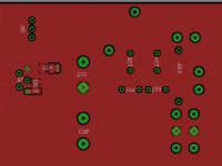
Following up on Eva's suggestion (and on IR's appnote) to use V- as plane for the output stage, would the attached layout be on track ? Or did I overlooked something ?
C203 is rail to rail, C13/14 are decoupling to rail, r32/c16 and r34/c15 are snubbers. Top plane is v-, bottom plane is 0V.
Following up on Eva's suggestion (and on IR's appnote) to use V- as plane for the output stage, would the attached layout be on track ? Or did I overlooked something ?
C203 is rail to rail, C13/14 are decoupling to rail, r32/c16 and r34/c15 are snubbers. Top plane is v-, bottom plane is 0V.
Attachments


I think this would fit to the concept of referencing the power plane to V-.
Where / how do you change over between V- plane and GND plane?
I think the entire driver section of the IRS2092 should be above the V- plane, while the small signal parts of the IRS2092 should be above GND plane.
How do you route the GND paths for the output filter, speakers and e-caps?
Where / how do you change over between V- plane and GND plane?
I think the entire driver section of the IRS2092 should be above the V- plane, while the small signal parts of the IRS2092 should be above GND plane.
How do you route the GND paths for the output filter, speakers and e-caps?

Analyze the current loops created.
- The ground of the electrolytics loops through power I/O connectors, this is series inductance. This could be tolerable as there is some ESR to damp the resonance, however there is a better option.
- The ground of C13 and C14 loops in the same way. This is going to ring, as ESR of ceramics is too low for the inductance of the plane going around.
My suggestion is:
- Move V+ trace near bottom edge of PCB. Rotate V+ electrolytic 180 degrees so that GND connection ends upwards.
- Place V- capacitor near V+ capacitor, so that ground interconnect is short.
- Move location for V+ to GND ceramic downwards near V- to GND ceramic, use vias to GND plane. I do not recommend populating the V+ capacitor. Place the V- to GND capacitor closer to electrolytics, then the V+ to GND closer to the FET.
- On top and to the right of electrolytics place output filter capacitors and RC, using close GND connection to the electrolytics.
- Place inductor on top of all, since nothing obstructs the routing.
- To ease the use of a raw piece of aluminum as heatsink the V+ to V- capacitor can be moved to underneath the V+ pin, and rotated 90 or 180 deg, as connection to V- through GND plane is low impedance
- For channel module PCBs I recommend adding at least ferrite beads to V+ and V- (or suitable small value, enough ESR, high current inductors), then another set of electrolytics and ceramics, this is to contain high frequency current from flowing through the wiring to power supply. Some RLC modelling including ESR of inductors and electrolytics is needed to do this right.
Agreed on that. That's what the app note is suggesting too. The difficult question is where and how to join the power ground plane and the top small signal groundplane.Where / how do you change over between V- plane and GND plane?
I think the entire driver section of the IRS2092 should be above the V- plane, while the small signal parts of the IRS2092 should be above GND plane
Thank you for the corrections. I tried to implement all of this in the attached layout. As before, top layer (red) is v-. As it is easier to not populate the ceramic cap from v+ to gnd than adding a pad afterwards, it's still onboard.- Move V+ trace near bottom edge of PCB. Rotate V+ electrolytic 180 degrees so that GND connection ends upwards.
- Place V- capacitor near V+ capacitor, so that ground interconnect is short.
- Move location for V+ to GND ceramic downwards near V- to GND ceramic, use vias to GND plane. I do not recommend populating the V+ capacitor. Place the V- to GND capacitor closer to electrolytics, then the V+ to GND closer to the FET.
- On top and to the right of electrolytics place output filter capacitors and RC, using close GND connection to the electrolytics.
- Place inductor on top of all, since nothing obstructs the routing.
- To ease the use of a raw piece of aluminum as heatsink the V+ to V- capacitor can be moved to underneath the V+ pin, and rotated 90 or 180 deg, as connection to V- through GND plane is low impedance
I also will use a form factor similar to ChocoHolic's, so I can quite easily raise the heatsink a few mm above the pcb.
There's some space freed at the bottom right of the pcb to add this filter. I'll see later on for that.- For channel module PCBs I recommend adding at least ferrite beads to V+ and V- (or suitable small value, enough ESR, high current inductors), then another set of electrolytics and ceramics, this is to contain high frequency current from flowing through the wiring to power supply. Some RLC modelling including ESR of inductors and electrolytics is needed to do this right
Attachments


- Home
- Amplifiers
- Class D
- SystemD LiteAmp