Hi there,
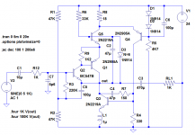
This buffer proves very difficult to stabilize. It is the result of a collaborative effort between Kenpeter and myself, and had never been tested IRL, just in sim.
Since I needed a high-perf buffer, I decided to give it a try.
It is based on well-known principles for this kind of circuits, ie. keeping all the conditions of the actual buffer element as stable as possible, but here this principle is pushed to the extreme.
The circuit is perfectly stable in sim, but my prototype oscillates madly.
The oscillation is a maximum amplitude squarewave of ~1MHz, which led me to think that the initial conditions triggered some kind of repetitive latch-up and let go, but it isn't the case: in fact, the cause is a VHF oscillation that builds up very quickly and ends up saturating everything, and upsetting DC bias-points.
What I have tried:
I tried to kill the bandwidth at every point possible; the only completely effective cure was a C-B cap of 10nF on Q2. Needless to say that it not only kills the oscillation but any usefulness as well.
The second best was a RC of 220ohm/47pF between the base of Q1 and the ground. I found this one by touching the point with a screwdriver, but it doesn't not remove the oscillation completely: it remains present as very short VHF bursts separated by a few ms, when the bias points have the time to settle.
Nothing else seems to have a positive effect.
In sim, I have tried to reproduce the effect by adding parasitics here and there, but I can only get an oscillation if I add a grossly exagerated parasitic cap (>15pF) in parallel with the 1µH (this one provides the compensation of the linearizing loop).
In general, I manage to tame even the most indocile beasts, but this one proves a tough nut to crack. The fact that the sim and prototype do not converge is problematic, because I built directly the definitive version, and making physical alterations is seriously unpractical.
One more detail, the prototype has been properly implemented from a physical point of view, with decouplings, shieldings, etc.
For my work, I routinely develop and build test-jigs good to 500MHz~1GHz, which means I know the rules and apply them properly.
Any ideas?
Attachments
Member
Joined 2009
Paid Member
No changeDoes it help to put a ferrite or resistor in base of Q3 ?
I already tried that, and most of the usual tricks tooSmall resistor in series with base of Q4 maybe..
Member
Joined 2009
Paid Member
The bootstrap is necessary for the high input impedance, but anyway the problem is present (under somewhat different forms) with both the input open or short-circuited to groundshould junction of R1 R2 be decoupled to ground instead of C5 bootstrap ?
No, because Q2 presents a negative input impedance at high frequencies and if the input protection R12 is alone, this does favor instabilities in sim.should there be a base stopper between C7 and Q2 ?
The effect is negligible due to the 220K already in series towards the baseTry to put in series with C5 resistor with value in order of 220-680ohm..
N=6 means 6 diodes in series.What's your practical implementation of D3 (N=6)? Is the sim reasonably robust against swapping out transistor models?.
Changing the transistor types for approximate equivalents changes nothing to the behavior of the sim (BC547-->2N3904, 2N2219-->2N2222, 2N2905-->2N2907)
Normally, yes, it is just in this case that such a big divergence appearsAre practical transistor Cs and stuff in reasonable agreement with the models?
Most of the problem is probably caused by the "vertical" (the current control) loop, but with interactions with the CFP that destabilizes it: I have just tried a feedforward cap between the collectors of Q3 and Q5, and 2.2nF is sufficient to stop the oscillations, but only with the input open.
When it is shorted, 100nF is required.
As I said above, I already tried all of the usual fixes, with no or little effectNot having read the whole thread, but did you try a gate stopper at Q4 and an R // L? That L probably has enough parasitic C to make it into a tank, should add some // losses.
Straight capacitance has apocalyptic effects, even in sim. A series RC brings some improvement, see above.Shunt compensation ,capacity from colector Q2 to ground, 330pF to 1nF?
Hi Elvee: How much current flows through Q2 and Q1?
I've used a reasonably similar output stage topology in which a high-IDSS NJFET was the input device rather than Q2 and Q1, Q4 operated as a phase-inverter, and Q3 was a PNP rather than a NPN.
Returning to the topology that you have, does decreasing the value of R9 accomplish anything useful?
kind regards, jonathan
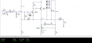
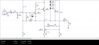
I was working on a buffer which operated close to the way this one does. It is very difficult to see what is happening using ltspice. I will show you using circuitmaker since it will show plainly the ac currents involved.
First using the schema attached we look at the ac current flowing out of the collector of Q3, 743.9uA. Next we look at the ac current flowing into the load, 707.1uA. As you can see there is more ac current flowing out of the collector of Q3, 36.8uA. Now as you will see this extra current is being driven into the collector of Q5, 14.8uA, and through capacitor C4, 21.57uA. If you look at the ac currents through the load, Q5, C4, the total equals the ac collector current of Q3. So it is driving itself.
First using the schema attached we look at the ac current flowing out of the collector of Q3, 743.9uA. Next we look at the ac current flowing into the load, 707.1uA. As you can see there is more ac current flowing out of the collector of Q3, 36.8uA. Now as you will see this extra current is being driven into the collector of Q5, 14.8uA, and through capacitor C4, 21.57uA. If you look at the ac currents through the load, Q5, C4, the total equals the ac collector current of Q3. So it is driving itself.
Attachments
The current in the main string, including Q2 is 30~35mA. Current through Q1 is ~0.7mAHi Elvee: How much current flows through Q2 and Q1?
.
I haven't tried this, but it will essentially increase the current through Q1, and therefore its transconductance, which is probably not desirable.Returning to the topology that you have, does decreasing the value of R9 accomplish anything useful?
I have tried shunting it with various capacitors, which reduces the magnitude of the impedance without increasing the first stage's transconductance, but to no avail
The AC values shown are just scalar, and tell nothing about the phase, or even just simply the polarities of the currents.I was working on a buffer which operated close to the way this one does. It is very difficult to see what is happening using ltspice. I will show you using circuitmaker since it will show plainly the ac currents involved.
First using the schema attached we look at the ac current flowing out of the collector of Q3, 743.9uA. Next we look at the ac current flowing into the load, 707.1uA. As you can see there is more ac current flowing out of the collector of Q3, 36.8uA. Now as you will see this extra current is being driven into the collector of Q5, 14.8uA, and through capacitor C4, 21.57uA. If you look at the ac currents through the load, Q5, C4, the total equals the ac collector current of Q3. So it is driving itself.
Since they are evaluated at 1KHz, I am pretty sure that the sums do add correctly, because the circuit has no built-in wideband negative resistance generation capability, unlike a lambda diode for instance.
If it were the case, Circuit-maker would show some kind of general oscillation like a multivibrator, which doesn't seem to be the case.
Here, the issue is a local negative resistance effect occuring at several tens of MHz, just like in a Colpitts oscillator for instance
Since you now have entered the schematic in Circuit-maker, with probably somewhat different models, could you check that the circuit is stable in transient mode at a high resolution (=small timestep in Ltspice)?
This will help to sort out the spice discrepancy issue
I haven't checked this specifically, but a base-stopper has basically the same effect, just marginally stronger, and it didn't prove useful.Final thought of the day")
Did anyone mention C6 ? How about trying a resistor in series with it.
I have also tried an emitter stopper (which has a much stronger effect in principle) in the form of a ferrite bead (=L//R), and it wasn't helpful either
Hi Elvee: The 1.2kohm value of R9 seems considerably higher than what I've had success with in output stage CFPs, but I haven't simulated to verify if that is a problem. The input CFP may also be more stable (in real life) is there is a ferrite bead inserted between the emitter of Q2 and the collector of Q1 / output.
My other suggestion - high IDSS NJFET input device, NPN or N-MOSFET cascode, then PNP phase-inverter and Q3 configured as a PNP emitter-follower, that topology I have shipped hundreds of units with nary a problem, so I know that would work. Doesn't need much in the way of compensation, either (only C7 as 15pF~33pF).
kind regards, jonathan
Last edited:
- Status
- This old topic is closed. If you want to reopen this topic, contact a moderator using the "Report Post" button.
- Home
- Amplifiers
- Solid State
- Unstable buffer