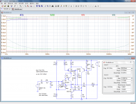
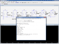
Here is the same analyzis using LT spice.I was working on a buffer which operated close to the way this one does. It is very difficult to see what is happening using ltspice. I will show you using circuitmaker since it will show plainly the ac currents involved.
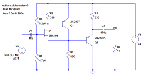
First using the schema attached we look at the ac current flowing out of the collector of Q3, 743.9uA. Next we look at the ac current flowing into the load, 707.1uA. As you can see there is more ac current flowing out of the collector of Q3, 36.8uA. Now as you will see this extra current is being driven into the collector of Q5, 14.8uA, and through capacitor C4, 21.57uA. If you look at the ac currents through the load, Q5, C4, the total equals the ac collector current of Q3. So it is driving itself.
I have used the AC analysis, because it didplays the phase too. At low frequencies, it is unimportant since it is always 0° or 180°, but at higher frequencies, working out intermediate phase values in transient mode is difficult.
To apply the Kirchoff's current law properly, you need to have the signs right, ie look at the current arrow on the component (depends how it is drawn) and the phase (0° or 180°) on the waveform viewer.
The following pic is the schematic annotated with these values for 1KHz.
The sum of the currents provided by the two active elements Q1 and Q3 is 1075µ. It is equal to the sum of the currents absorbed by the main passive elements, load, bootstrap, etc.
Q3 provides the brunt of the current, which is normal: that is the purpose of this circuit. The 1050/25 ratio is the loop gain of the circuit, Q1 is just the steering device.
If negative resistance was apparent at the collector of Q3, it would result in a negative current into Q1, which would cause instabilities and is obviously not the case here, particularly at 1KHz where no problem is observed.
With this sim, even at higher frequencies no instabilities occur, unlike the physical circuit.
Attachments
I think I have already tried that, but I will retry anywayHi Elvee: The 1.2kohm value of R9 seems considerably higher than what I've had success with in output stage CFPs, but I haven't simulated to verify if that is a problem. The input CFP may also be more stable (in real life) is there is a ferrite bead inserted between the emitter of Q2 and the collector of Q1 / output.
Could you post a schematic, I 'll simulate it, but I have doubts: jFETs have a high distortion compared to BJT's, and here I need ppb level up to 100KHz, which seems difficult to achieve with FETs.My other suggestion - high IDSS NJFET input device, NPN or N-MOSFET cascode, then PNP phase-inverter and Q3 configured as a PNP emitter-follower, that topology I have shipped hundreds of units with nary a problem, so I know that would work. Doesn't need much in the way of compensation, either (only C7 as 15pF~33pF).
Greetings Elvee: A PNP can be combined with the input N-JFET to make a CFP, which should push the distortion farther down.
However, ppb will be difficult, not only regarding the schematic but also the physical build (but I know that you are well aware of that).
Regarding schematics, I post here so little these days that I have completely forgotten how to attach a graphic to a post, and how to extract a graphic from a pdf (sheepish grin). If you could send me a PM or email, I'd be pleased to email you a pdf schematic.
kind regards, jonathan
Greetings Elvee: A PNP can be combined with the input N-JFET to make a CFP, which should push the distortion farther down.
Is this what you have in mind?
Attachments
Hi Elvee: Regarding a JFET CFP, yes, something like that may do (although I have neither simulated nor built your device choices).
May I assume that the sole purpose of the latest schematic that you posted is to show some kind of JFET CFP being used as the input device for a buffer? The complete buffer that I have in mind is very different from the latest schematic (and much closer to your first schematic).
kind regards, jonathan
Q4 operated as a phase-inverter
Hello Jonathan, what is the input signal and where the output of phase inverter is applied?
Hi Dimitri: Long time no speak ") !
!
>what is the input signal?
Input signal would be the same as V3 in Elvee's schematic. With rail voltages of +/-22V, the input level will be OK up to 10~11V (output won't begin to clip).
>where the output of phase inverter is applied?
The collector of Q4 continues to control Q3's base, except that Q4 is configured as a phase inverter rather than a folded-cascode, and Q3 becomes a PNP follower. R4 becomes a constant-current sink (or a moderately high-value resistor).
So, collector of Q2 inverts phase, phase inverter Q4 brings phase back, and Q3 follows. This allows the emitter of Q3 to form the signal output node along with the emitter of Q2. All component identifiers are referred to Elvee's initial circuit.
I've been building these with JFET inputs, and cascoding for Q3 as well as cascoding Q2 with Q5 (again referring to Elvee's schematic), but the core concept is the same as the circuit that John Broskie (11 years) later called the "Triadtron".
http://tubecad.com/2010/05/17/Triadtron at last.png
Triadtron
Aikido Cathode Follower & More Triadtron
It's About Time&Ultra-Linear Line Stages
Might Diamonds
Feel free to pm me or email me if you wish.
kind regards, jonathan
!>what is the input signal?
Input signal would be the same as V3 in Elvee's schematic. With rail voltages of +/-22V, the input level will be OK up to 10~11V (output won't begin to clip).
>where the output of phase inverter is applied?
The collector of Q4 continues to control Q3's base, except that Q4 is configured as a phase inverter rather than a folded-cascode, and Q3 becomes a PNP follower. R4 becomes a constant-current sink (or a moderately high-value resistor).
So, collector of Q2 inverts phase, phase inverter Q4 brings phase back, and Q3 follows. This allows the emitter of Q3 to form the signal output node along with the emitter of Q2. All component identifiers are referred to Elvee's initial circuit.
I've been building these with JFET inputs, and cascoding for Q3 as well as cascoding Q2 with Q5 (again referring to Elvee's schematic), but the core concept is the same as the circuit that John Broskie (11 years) later called the "Triadtron".
http://tubecad.com/2010/05/17/Triadtron at last.png
Triadtron
Aikido Cathode Follower & More Triadtron
It's About Time&Ultra-Linear Line Stages
Might Diamonds
Feel free to pm me or email me if you wish.
kind regards, jonathan
When creating ASCII net lists (typing into a text editor) for SPICE simulators, M=43 means 43 copies of this element in parallel, whether the element is a BJT, FET, diode, resistor, capacitor, inductor, or subcircuit instantiation. ("M" abbreviates "multiplicity".) I'm surprised to read that you are quite certain you're getting N=6 diode elements in series. Is the "N" parameter (series) exactly the converse of the "M" parameter (parallel)?
What do you think happens when you attach N=43 to a three terminal element like a MOSFET? If you get 43 MOSFETs in series, where do the 43 different gate nodes connect? And how does it work for a 7-terminal sub circuit instantiation?
What do you think happens when you attach N=43 to a three terminal element like a MOSFET? If you get 43 MOSFETs in series, where do the 43 different gate nodes connect? And how does it work for a 7-terminal sub circuit instantiation?
Last edited:
What do you think?What do you think happens when you attach N=43 to a three terminal element like a MOSFET?
See here:
Attachments
In my limited view, the double-side Sziklai formation with the 3 transistors won't be doing exactly the same as the LTP-looking 2 transistor differential function above them, and therefore this circuit wants to go in a direction (amplify either positive or negative), which is not conducive to zero gain (the reaction to both sections for DC is the same, but for AC could not possibly be the same). That may be an excellent amplifier that doesn't want to be a buffer. It may be possible to block undesired powerside communication with a voltage drop and load (dc for voltage drop, ac for following load), such as either a CCS or a diode with the output end loaded by a charged up ~100uF cap (repeated for each connection to any rail) so that excess signal doesn't traverse the rails between points in the circuit. My post was guesswork. But, I do think that a transistor is missing, because on appearance alone, it doesn't look like it can do equal and opposite gain for signals. I guess that there may be a resistor where a transistor should be--one of the resistors is unfortunately bidirectional and needs replaced with something that can't do that.
Sorry that it was the extent of my best guess.
Sorry that it was the extent of my best guess.
Or, to shorten that, it has either one too many transistors, or lacks for one more transistor. I think that if a buffer has an unequal number of transistors then a battle is requested because that also means an unequal number of resistors, which cannot inherently measure a voltage and therefore causes a battle when one wants a zero gain factor.
This buffer is a building block of a high resolution audio measurement system, and it will have to process a range of frequencies centered around ~100KHz with sub-ppm linearity, ideally sub-ppb, hence the "complexity" (which is quite relative and moderate considering the performances)It's a BUFFER for goodness sake. Why the 'faux arte' complexity?
It is a microchoke from Epcos. Its // capacitance is a few pF's, and the SRF must be around 100MHz.What is the quality of L1? Resonances maybe?
Yes, it changed nothingDid you try parallel resistor?
If it helps, just by playing around with your circuit trying to make it oscillate in LTspice using possible stray capacitance and wiring inductance values, a 20pF or higher capacitance between Q5 collector and the output combined with 100nH between the top of R8 and D1 in the +ve supply line induces VHF oscillation.
Playing around again but this time to try and stop the oscillation with as low a value cap as possible, the most effective place was 15pF between Q2 base and Q5 emitter.
Playing around again but this time to try and stop the oscillation with as low a value cap as possible, the most effective place was 15pF between Q2 base and Q5 emitter.
Divide and Conquer?
Perhaps simplifying the circuit to get some data would be helpful.
SWAG-the bias loop Q4-Q3 thru the main amp xistors (Q2-Q1) up through Q5 could be unstable.
What if, just as an experiment to test that theory, you broke that loop? Simplest way that preserves the most parasitics, might be to
1. temporarily short out D1 and D2
2. place a 500 Ohm resistor from the out node to ground to get pull down current.
If it stabilizes things, it might give you a hint as to where to go next.
- Status
- This old topic is closed. If you want to reopen this topic, contact a moderator using the "Report Post" button.
- Home
- Amplifiers
- Solid State
- Unstable buffer